


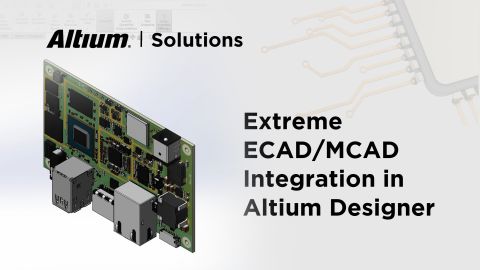


How to Use ECAD-MCAD Co-Design for PCB Enclosure Design and Board Layout

At a Glance
Ensure seamless PCB-to-enclosure fit with ECAD-MCAD integration. Prevent interference, optimize design, and streamline multi-board workflows.


Printed circuit boards are fun to design and lay out, but a PCB will need an enclosure to hold it mechanically stable. PCB enclosures can be purchased off-the-shelf, or you can create a custom enclosure design using MCAD software. No matter which route you take to create your enclosure, you’ll need to import your PCB layout into MCAD tools to ensure your board and components will not interfere with the enclosure.
When you’re working with a complex layout, multi-board system, or flexible PCB, you’ll need to quickly access MCAD software to inspect interference between your PCB enclosure design, your electronic components, and your board. Altium contains the MCAD tools you need to check mechanical interference as you design your circuit board and your custom enclosure design, and it includes the most powerful set of circuit board design features. Designers can create complex boards for any application alongside their enclosures.
How to Design a PCB Enclosure and a Layout to Prevent Interference
When you need to design an enclosure around your PCB layout and prevent interference between components, you have a few options to help ensure accuracy in your design:
- Export your PCB layout as a STEP file and import it into an MCAD application for enclosure design
- Export your enclosure as a STEP file and import it into your ECAD software
Altium supports both processes as part of PCB layout and enclosure design. However, when you need to prevent interference, you can import a STEP file into your PCB project and check for interference manually or automatically. Design rule definitions can be used to check the component placement for interference with a PCB enclosure in 3D to identify when parts on the PCB need to be moved.

Clearance and collision checking in 3D with Altium
Unfortunately, PCB designers need mechanical engineers or MCAD software in order to make changes to an existing enclosure or design a custom enclosure for a PCB. These enclosure designs demand an ECAD-MCAD co-design approach between the electrical and mechanical disciplines.
Custom PCB Enclosure Design Demands ECAD-MCAD Collaboration
For many products, creating the desired user experience demands co-design between mechanical and electrical designers. The interplay between the mechanical and electrical engineering domains gives two approaches for defining constraints in the design space.
- Mechanical-First Approach: The desired enclosure is determined first and used as the main constraint for board size, component sizes, and component placements.
- Electrical-First Approach: The PCB size is determined first, sometimes only being finalized after a layout is finished. Once the layout is done, the mechanical engineer builds around the PCB.
The electrical-first approach is much easier because it gives the electrical engineer all the freedom to select and place parts around the PCB layout. Once that is completed, the mechanical engineer takes a finished design model and builds the custom enclosure design around it. This is essentially a waterfall approach that takes us back to the days of over-the-wall engineering.
These designs might look simple, and the custom design tends to look like a box, essentially surrounding the PCB components with a minimum margin for the enclosure walls.
When a more unique functional and aesthetic experience is required in the products, the mechanical-first approach dominates. That means design teams will need a co-design approach where constraints are initially defined in MCAD software rather than in the PCB layout.
MCAD Co-Design for PCB Enclosures
An important process for developing PCB enclosures is MCAD co-design, where mechanical and electrical designers iterate back and forth to develop a PCB and its enclosure. The process is used with complex PCB enclosures, which may have complex shapes and may even integrate multiple PCBs into the same assembly.
For mechanical engineers, MCAD co-design approaches provide many benefits, with the most important being the ability to define the constraints for the electrical designer. Placing constraints on the PCB layout means setting several elements that are needed for the PCB to mount and fit the enclosure, such as:
- Overall PCB size and dimensions
- Total PCB thickness
- Location of keepouts, including height-based keepouts
- Location of mounting holes, cutouts, or slots
- Placement of specific components, typically connectors
- Planning and modeling of wiring and cable routes
Planning these elements first does constrain the board designer, but it also ensures that their design will fit within the desired enclosure. Typically, after placement, a 3D model of the PCB with its components is reviewed in order to check fit to the enclosure.

Enclosure clearances and interference can be checked in 3D using Altium’s integrated MCAD toolset.
With these constraints defined, the mechanical engineer can focus on building the enclosure and planning for its fabrication process. Meanwhile, the PCB designer can focus on building a PCB layout that sits within these constraints. Periodic reviews of the component placement will be necessary to ensure the mechanical constraints are not violated in the PCB layout. This can be done with the standard push-pull process via a cloud platform like Altium.
Off-the-Shelf PCB Enclosures
There are many off-the-shelf options for PCB enclosures with a variety of features. This makes off-the-shelf enclosures useful in many settings, particularly in the case of prototyping or quick-turn production at low to moderate volume. These off-the-shelf enclosures provide a quick go-to-market option that is adaptable for many designs. These enclosures are often complete with mounting posts, talking holes, threaded holes for fasteners, openings for cabling or connectors, and vents for airflow. Some off-the-shelf enclosures may also have a high IP rating, and when combined with a similarly rated panel-mount or chassis-mount connector, they enable a high-reliability system that can withstand the elements.
An example PCB enclosure from Polycase is shown below. These enclosures are suitable for many designs, including digital systems, embedded systems, and small power electronics systems.

Vendors of off-the-shelf enclosures for PCBs typically provide a 3D mechanical model of the enclosure, which can be used to define constraints for the PCB. Using a 3D model for the enclosure and exporting a 2D outline for the board follows the MCAD-first approach for designing with a PCB enclosure and requires an MCAD software package. Based on the 3D model, the MCAD designer can trace out a PCB outline that will fit within the enclosure and conform to any mounting posts or standoffs. CAD users can also provide a board thickness specification inside the enclosure model and hand this information off to the PCB designer.
While handing off a DXF is often the standard approach to defining the board geometry, MCAD software users can also push the board geometry directly into ECAD software like Altium. Direct push into the PCB eliminates the file exchange and ensures the designer always has the correct mechanical specification for the PCB.
ECAD-MCAD Collaboration with Altium
Altium transforms ECAD-MCAD collaboration by providing a unified cloud platform that eliminates traditional file exchange bottlenecks. The platform enables real-time synchronization between electrical and mechanical design teams, with seamless sharing of PCB layouts, component models, and enclosure constraints.
Mechanical engineers can push board geometry specifications directly into Altium. Electrical engineers can share updated layouts without manual file transfers. ECAD and MCAD integration supports iterative co-design that simplifies the design of complex enclosures.
Working with Complex 3D PCB Layouts in Altium
When you’re working with a complex layout, multi-board system, or flexible PCB, you’ll need to quickly access MCAD tools to inspect interference between your PCB enclosure, your electronic components, and your board. Altium contains the ECAD and MCAD tools you need to check mechanical interference as you design your circuit board and your enclosure, and it includes the most powerful set of circuit board design features. Designers can create complex boards for any application alongside their enclosures.
Altium is the only PCB design platform that provides a complete set of ECAD and MCAD features for any electronics application. Whether you’re designing simple PCBs or complex multi-board systems, Altium has the electrical and mechanical design features you need to create cutting-edge technology.
Altium brings an unprecedented level of integration to the electronics industry, previously seen only in software development, enabling designers to collaborate securely and reach unprecedented levels of efficiency.
Ready to optimize your ECAD-MCAD workflows? Start collaborating today!

关于作者
Related Technical Documentation
相关资源
目录
从设计到发布,全程无阻碍
- 让评审始终关联到正确的版本
- 减少交接中的混乱和返工
- 更早发现采购与发布风险
- 可独立工作,按需共享
开始使用
Thank you, you are now subscribed to updates.

 沪公网安备 31010502006411号