


Create PCB Data Management System Structures in Altium Designer

At a Glance
Your PCB data management system structures help you stay organized and keep current data in your PCB designs.


In what some refer to as the “Olden Days” of the electronics industry, there wasn’t much need for PCB data management. Tasks like creating schematics, BOMs, drawings, and Gerber files were problematic. Today, the PCB design industry has seen major advancements in technology, driven by what can only be described as an insatiable hunger by consumers for faster, smaller, and sleeker products with all the latest technology and functions.
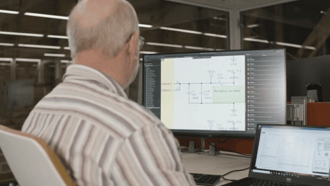
Today’s PCB data management tasks are aided by PCB design software like Altium Designer. With this powerful platform, you can easily track, share, distribution, and maintenance of all the data connected to the development of printed circuit boards or PCBs. Here’s why you need to use the integrated design and PCB data management environment in Altium Designer and how these data management features help prevent design and production errors.
ALTIUM DESIGNER
A comprehensive software package that allows design teams to create PCB data management system structures in their libraries.
In the world of modern electronics, there is a huge drive for shorter product development times with greater product complexity and more functions. Design teams need to get it right the first time if they want to get to market quickly and have an edge over competitors. This requires coordinated action between everyone from end customers to design teams and manufacturers.
The days of being able to design, fabricate, assemble and test multiple spins of the same PCB assembly with no clear results or benefits are over. Getting to manufacturing quickly requires keeping track of your component specifications, sourcing information, and PCB design data in a single place. This is where the integrated libraries in Altium Designer are ideal for PCB design data management and for preparing for production.
What is PCB Data Management?
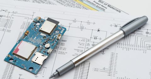
A single electronic component now has endless information attached: electrical parameters, sourcing information, lifecycle status, 3D models, compliance certificates, datasheets, and much more. This information is always changing, and designers need to have tools to keep their information up to date. PCB data management requires keeping your design data singular in nature. In other words, it’s all about organizing and tracking components, schematics, and PCB layout data in a single repository so that they can be easily accessed and reused when needed.
How to Understand Complex PCB Data Management System Structures
PCB data management can be difficult for several reasons. Many times, it is because design teams are not tracking PCB design data using the same naming conventions or repositories. In other cases, design teams simply don’t have access to design tools that help centralize data while keeping backups and providing revision tracking. The right set of PCB design tools will help you track and manage your component libraries and the data they contain.
- When your PCB design software fetches data updates from component repositories, you can keep your component libraries and your designs updated without manually searching for the latest footprints.
See how automatically updating component libraries keep you organized.
- The best data management software will take your component data and import it into your bill of materials when preparing for manufacturing.
See why your PCB design software needs bills of materials management features.
- The right set of sourcing tools will integrate with your PCB design software, allowing you to create component libraries with complete PCB CAD data and sourcing information.
Learn more about sourcing components with Octopart’s Christopher Calvi.

The unified PCB data management platform in Altium Designer imports your component data into a bill of materials.
Tools for PCB Design Data Management
The biggest problem in PCB data management is not the amount of information that needs to be tracked, but how your structure a system and processes for managing all of it. If the right data is not readily available to those who need it, any data management system will be useless. To take something that is complex or overwhelming and maybe difficult, break it up into small manageable parts and simply deal with each piece.
Creating a PCB Data Management Workflow
Your data management workflow requires centralization and tracking of data in standard file formats, but the data in your component libraries need to be accessible in your PCB design software. This allows you to instantly import your component data into your design data, and your components will be correct across all your designs.
Once you need to produce your board at scale, your design data management features should integrate with your manufacturing deliverable tools. When your PCB design data is placed in a centralized location and tracked with the best version control tools, you can ensure your production data remains current and your design data does not include any errors.
- A workable data management process has the right architecture for helping you remain productive.
Learn more about the best architecture for managing component data.
- Now you can access insights into the industry’s best data management practices for large PCB design teams.
See how industry leaders are managing their component and design data.
- An important part of PCB data management is access to updated supply chain information to spot obsolete components, current stocks, lead times, and prices.
See how you can stay on budget with the right PCB data management tools.

The design tools in Altium Designer unify your component and design data to ensure all your designs are correct.
Create Your PCB Data Management System in Altium Designer
All the data management features you need to track component specifications, retrieve updated sourcing information, and download new components can be found in Altium Designer. Your design team won’t have to constantly rebuild components, search distributor websites for sourcing data, or create disparate PCB data management systems. Altium Designer includes all these features alongside the industry’s best CAD tools for PCB design.
Unified PCB Design and Data Management in Altium Designer
The design interface integrates all your design tools with your component libraries and centralized data management tools, which help prevent component data errors and keep your team productive. When you’re ready to produce your board at scale, your data management tools will integrate with your PCB manufacturing tools, allowing you to create deliverables for your new board.
- With Altium Designer, your design tools are integrated alongside your PCB design and component library management features. Design teams can create PCB data management system structures to stay productive.
Learn more about the unified design environment in Altium Designer.
- Altium Concord Pro is a unique PCB data management tool that integrates with Altium Designer. Your team can easily track project lifecycles and share component data through Altium Designer and a convenient web interface.
Learn more about unifying Altium Concord Pro with Altium Designer.
- The management and collaboration features in the Altium 365 platform give you the tools you need to create PCB data management system structures for your design team.
Learn more about the PCB data management tools in Altium 365.

The unified PCB data management and design view in Altium Designer
Quickly creating your PCB design requires ensuring you remain organized with consistent PCB data management system structures. The library and component management tools in Altium Designer are ideal for creating a productive workflow for your team, and they help you get to manufacturing without delays.
Altium Designer on Altium 365 delivers an unprecedented amount of integration to the electronics industry until now relegated to the world of software development, allowing designers to work from home and reach unprecedented levels of efficiency.
We have only scratched the surface of what is possible to do with Altium Designer on Altium 365. You can check the product page for a more in-depth feature description or one of the On-Demand Webinars.

关于作者
Related Technical Documentation
相关资源
目录
从设计到发布,全程无阻碍
- 让评审始终关联到正确的版本
- 减少交接中的混乱和返工
- 更早发现采购与发布风险
- 可独立工作,按需共享
开始使用
Thank you, you are now subscribed to updates.

 沪公网安备 31010502006411号