


Rigid-Flex PCBs in Consumer Electronics

At a Glance
Explore how rigid-flex PCBs for consumer electronics improve reliability and 3D integration in modern devices. Learn key design rules, trends, and workflow best practices.


Consumer devices keep getting thinner, lighter, and more mechanically complex, pushing more products toward rigid-flex PCB architecture. Rigid-flex lets you place high-density electronics where they belong, then route through tight corners, wraps, or constrained 3D cavities without filling the enclosure with connectors and cabling. When you treat bend regions, stackups, and manufacturing communication as first-class constraints from the start, rigid-flex becomes a repeatable approach rather than a one-off risk.
Key Takeaways
- Rigid‑flex is now a mainstream packaging strategy in consumer electronics, driven by thinner devices, complex 3D enclosures, and the need to reduce connectors while improving reliability in small, multi‑zone architectures.
- Successful rigid‑flex design depends on early definition of bend zones, regional stackups, and transition details, since mechanical strain, bend radius, and copper layout constraints largely determine long‑term durability.
- Flex regions require different design rules than rigid areas, including conservative routing, careful component spacing, and strict avoidance of copper near bend starts—common failure points in consumer rigid‑flex builds.
- Market trends like AI glasses, advanced wearables, Ultra‑HDI routing, and thermoformed flex are expanding rigid‑flex adoption, but also increasing the importance of disciplined, manufacturer‑aligned design workflows and early mechanical collaboration.
Where Rigid-Flex Is Used in Consumer Electronics
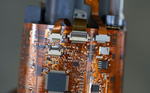
Rigid-flex combines rigid and flexible circuit sections into a single fabricated unit, allowing it to fold or route through limited geometry. In consumer electronics, that translates to better packaging efficiency and fewer connectors, reducing stress on discrete cabling during motion and handling.
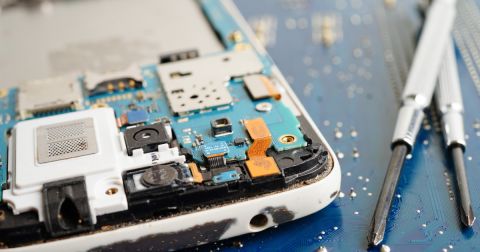
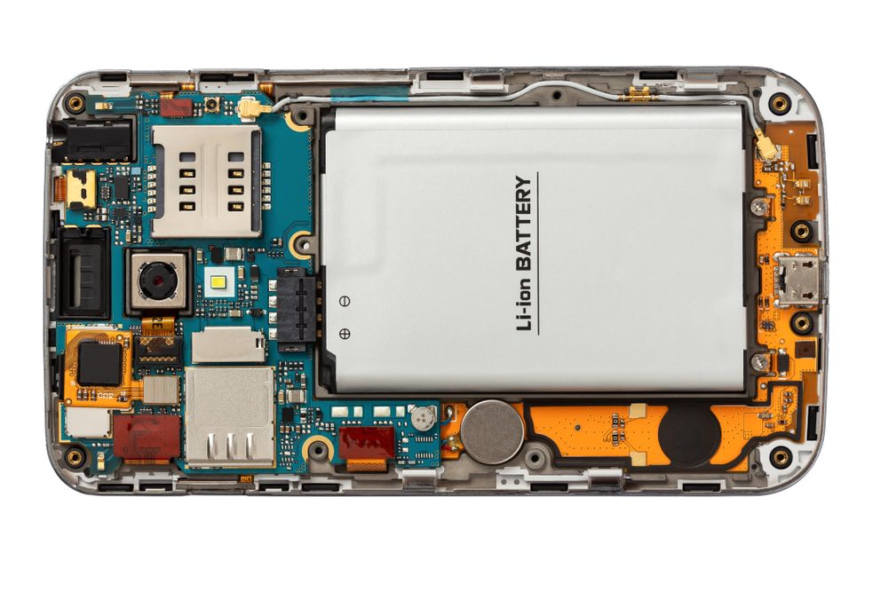
Smartphones and Foldables
Phones remain the volume driver for flexible PCB usage, and rigid-flex PCBs align well with how phones are physically assembled: multiple functional zones, tight cavities, and interconnects that can withstand handling, shock, and in some cases, hinge motion. Taiwan Printed Circuit Association (TPCA) and Industrial Technology Research Institute (ITRI) outlook (as reported by I-Connect007) describes mobile phones as the largest application category for flexible PCBs.
Foldables intensify these demands. You split the system across multiple rigid zones and route signals and power through a tight hinge region, where bend-zone definition and transition discipline determine long-term reliability.
Wearables: Watches, Rings, Patches, and IoT Form Factors
Wearables force electronics into shapes that are difficult for traditional rigid boards, including curved housings, strap geometries, skin-contact zones, and tiny internal volumes. EMI, antenna routing, and thermal behavior can become system-level risks in these devices because the mechanical context is unforgiving.
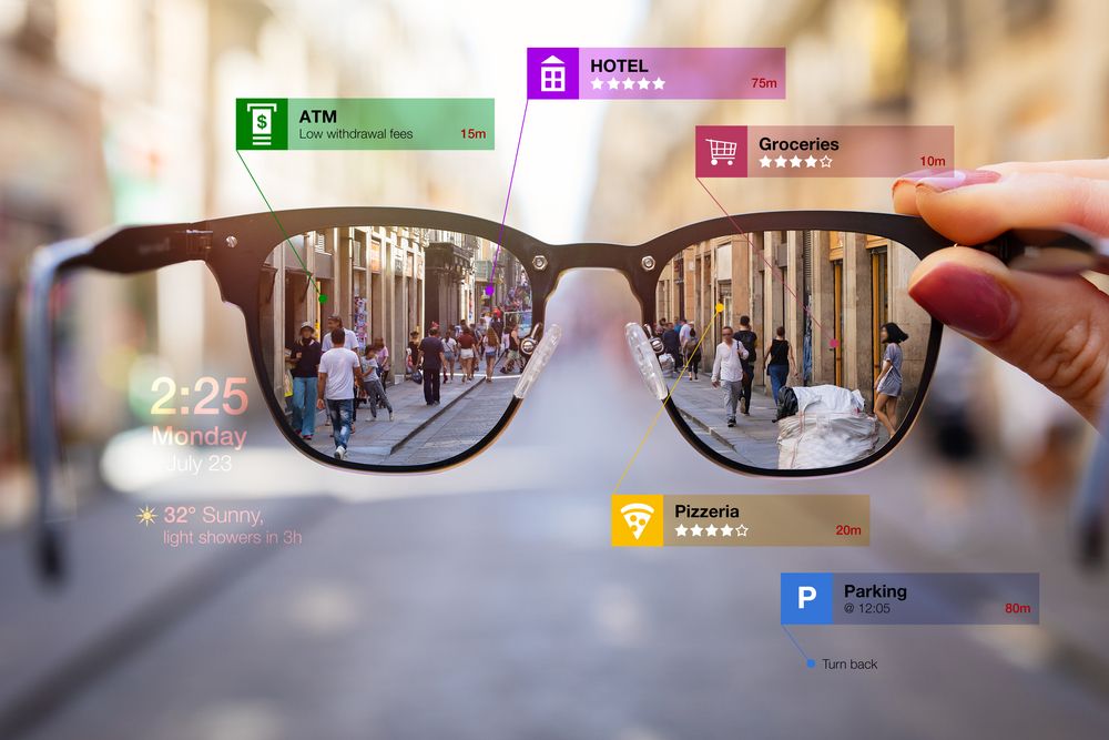
Smart Glasses and AR Glasses
Smart glasses are a classic rigid-flex use case: limited temple volume, tight Z-height, and a need to distribute electronics across separated regions while maintaining comfort and balance. TPCA and ITRI’s 2025 outlook highlights AI glasses as an emerging growth driver. Altium’s component-level overview of smart and AR glasses covers the packaging limitations of fitting dense sensing, displays, power, and connectivity into a wearable industrial design.
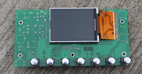
Compact Camera and Module-Style Architectures
Module-driven consumer architectures often benefit from rigid-flex when you need a mechanically space-limited module, such as a camera, sensor cluster, or small compute island, that still needs high-integrity routing into the rest of the device. A rigid island provides stable component mounting and controlled geometry, while the flex section routes through tight cavities without adding connectors and extra assembly steps. Treat the transition into the module like a reliability boundary. Define strain relief, and keep copper features away from the bend start.
What Changes When You Move from Rigid to Rigid-Flex
Rigid-flex changes your risk map:
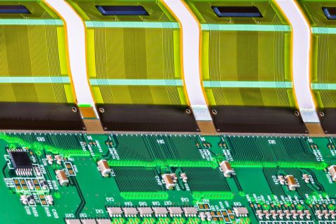
Bend Zones Are Engineered Regions
Flexible circuit design is limited by mechanical factors, including bend radius, copper strain, layer construction, and whether the bend is static (bend-to-fit) or dynamic (repeated flex). To manage these constraints, define bend zones early and plan for strain relief near rigid region edges.
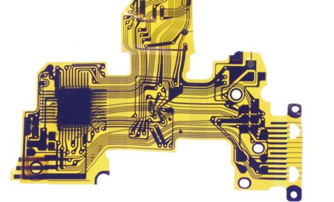
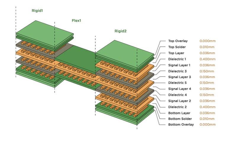
Stackups Become Multi-Zone by Default
Rigid-flex does not use a single stackup for the rigid region, which allows definition of stiffener regions and integrated flex regions. That drives how you document the build. Fabricators need clear layer naming, material callouts, and transition details so they can interpret exactly where each construction starts and ends.
Assembly Rules Change: Component Placement and Reliability
Placement near bend regions allows mechanical strain to propagate to solder joins in the assembly. Allow sufficient spacing between bend regions and SMT parts that are placed on flex areas. In addition, use prototyping or simulation to validate bend behavior and to confirm thermal and mechanical reliability.
Common Failure Patterns Are Predictable
Flexible circuit projects often fail in predictable ways, from misunderstanding bend requirements to placing features too close to bend transitions. Check the top 10 common flexible circuit design mistakes to understand how treating the bend start like ordinary routing space is one of the fastest ways to create a late failure.
The Trends Designers Should Track
AI Glasses and New Wearables Are Accelerating Demand
TPCA and ITRI's outlook projects the 2025 flex PCB market size at US$20 billion, with a 6.4% annual growth rate over 2024, driven increasingly by AI glasses.
Ultra-HDI Meets Flex Constraints
Consumer devices are tightening routing density, pushing more designs toward Ultra-HDI features such as finer lines, smaller vias, and denser interconnects. That helps you fit more functionality into less area, but it also raises the bar for rigid-flex discipline. Higher density can collide with bend reliability because thinner structures, tighter geometries, and aggressive transitions are less forgiving in flex regions. Concentrate Ultra-HDI where the board stays rigid, then keep flex regions mechanically conservative and manufacturer-aligned to avoid trading packaging wins for yield or reliability surprises.
Thermoformed Flex Are Expanding the Design Space
Rigid-flex is no longer the only way to go 3D. Thermoformed flex techniques offer paths to permanently shaped circuits and embedded electronics in consumer-relevant form factors.
A Practical Workflow Using Altium Develop
- Start with the Mechanical Envelope, Then Lock the Regions
a. Define rigid zones, flex zones, and no-feature constraints early, based on the enclosure and motion model.
b. Treat bend areas as first-class design elements, not leftover whitespace.
- Build Multi-Zone Stackup Intent Up Front
a. Establish the master layer model, then derive regional constructions (rigid, flex, stiffened flex) from it.
b. Document coverlay, adhesives, stiffeners, and region transitions explicitly.
- Encode Bend and Transition Rules, Then Route Inside the Rules
a. Favor rule-driven checks for bend-area behavior, including trace orientation expectations, width change limits, and keepouts from bend starts.
- Validate Assembly Reality Early
a. Prototype flex assemblies to validate the combined mechanical, thermal, and bending stresses.
- Generate a Fabrication Package That Communicates Intent
a. Align early with your fabricator, especially on stackup feasibility and bend reliability targets.
The Real Takeaway for Your Next Consumer Build
As industrial design forces electronics into multiple planes and tighter volumes, rigid-flex has become a mainstream packaging tool for consumer products. The penalty for vague assumptions is higher than with rigid boards, because bends, transitions, and region stackups amplify small mistakes.
Use the Altium Develop to define bend zones, regional stackups, and the release package as explicit, rule-checked parts of the design, then carry them through layout, 3D validation, and documentation. Do that consistently, and rigid-flex becomes predictable and scalable across product lines.
Whether you need to build reliable power electronics or advanced digital systems, Altium Develop unites every discipline into one collaborative force. Free from silos. Free from limits. It’s where engineers, designers, and innovators work as one to co-create without constraints. Experience Altium Develop today!
Frequently Asked Questions
What are the most common failure points in rigid‑flex PCB designs?
The most frequent failures occur at rigid‑to‑flex transitions, where copper features or vias are placed too close to the bend start. These areas experience high mechanical strain, especially in dynamic‑flex applications. Inadequate bend‑radius planning, insufficient strain‑relief patterns, and ignoring layer construction constraints also increase the risk of cracking or delamination.
How do I choose the correct bend radius for a flexible circuit?
Bend radius depends on factors like copper thickness, number of layers, type of flex (static vs. dynamic), and materials used. As a rule of thumb, dynamic flex regions require significantly larger bend radii. Designers should follow IPC‑2223 guidelines and consult their fabricator early, since incorrect bend-radius assumptions can lead to premature mechanical failure.
Why is early stackup definition critical in rigid‑flex PCB development?
Rigid‑flex boards use multi‑zone stackups, meaning rigid, flex, and stiffened areas each require separate constructions. Early stackup definition ensures proper coverlay placement, adhesive layer configuration, and clear documentation for the fabricator. This helps avoid misinterpretation, lowers manufacturing risk, and improves long‑term reliability.
When should Ultra‑HDI features be used in consumer rigid‑flex designs?
Ultra‑HDI routing (finer lines, microvias, and higher interconnect density) is best used in rigid regions, where the structure can support tighter geometries. Flex regions should remain mechanically conservative, since extremely thin or dense features reduce bend reliability. Designers often apply Ultra‑HDI only where needed for components, while keeping flex areas optimized for durability.

关于作者
Related Technical Documentation
相关资源
目录
- Key Takeaways
- Where Rigid-Flex Is Used in Consumer Electronics
- Smartphones and Foldables
- Wearables: Watches, Rings, Patches, and IoT Form Factors
- Smart Glasses and AR Glasses
- Compact Camera and Module-Style Architectures
- What Changes When You Move from Rigid to Rigid-Flex
- Bend Zones Are Engineered Regions
- Stackups Become Multi-Zone by Default
- Assembly Rules Change: Component Placement and Reliability
- Common Failure Patterns Are Predictable
- The Trends Designers Should Track
- AI Glasses and New Wearables Are Accelerating Demand
- Ultra-HDI Meets Flex Constraints
- Thermoformed Flex Are Expanding the Design Space
- A Practical Workflow Using Altium Develop
- The Real Takeaway for Your Next Consumer Build
- Frequently Asked Questions
- What are the most common failure points in rigid‑flex PCB designs?
- How do I choose the correct bend radius for a flexible circuit?
- Why is early stackup definition critical in rigid‑flex PCB development?
- When should Ultra‑HDI features be used in consumer rigid‑flex designs?
从设计到发布,全程无阻碍
- 让评审始终关联到正确的版本
- 减少交接中的混乱和返工
- 更早发现采购与发布风险
- 可独立工作,按需共享
开始使用
Thank you, you are now subscribed to updates.
 沪公网安备 31010502006411号