


Design Your Small Circuit Board in Altium Designer


Large circuit boards, small circuit boards, and anything in between might seem like they need separate sets of PCB layout features. In reality, your PCB design software shouldn’t delineate your PCB design based on size. Whether you need to design a large or small circuit board, a design application with high-quality CAD tools will help you get the job done quickly and prepare your board for production.
Small circuit board designs are much easier to create when you use high-quality CAD tools like the kind you’ll find in Altium Designer. The PCB design and layout features in Altium Designer are adaptable to boards of any size, shape, thickness, copper weight, and material. In addition, the DRC engine in Altium Designer helps ensure your layout complies with basic electrical and mechanical design rules. Here’s how you can design high-quality circuit boards of any size with Altium Designer’s complete set of PCB design tools.
ALTIUM DESIGNER
The only PCB design package for large and small circuit boards, as well as high-density layout and routing for a range of electronics applications.
As a circuit board gets smaller, component layouts get tighter, and routing becomes denser. To prevent problems with signal integrity, shorts during assembly, mechanical interference, and dense routing, designers need full control over their design rules and layout tools. Some design programs enforce the same rules, routing settings, clearance settings, and stackup limitations for every circuit board, regardless of its size.
Altium Designer is different. The layout and routing features in Altium Designer were created to work with circuit boards of any size and density. Designers have full control over an online DRC engine, which allows a designer to specify application-specific design rules for small, high-density circuit boards. When you need to take control over design and layout of a small circuit board, look to the design tools in Altium Designer.
Getting Started With Small Circuit Board Design
There is no specific size that qualifies a circuit board as “small,” but smaller PCBs tend to have some common characteristics:
- They tend to use smaller surface mount components (0402, 0201 packages are common)
- Density tends to be higher and trace width tends to be smaller
- Integrated circuit packages tend to be smaller
- Board shape and thickness may be non-standard
- Via and mounting hole sizes tend to be smaller
- Tracks between components tend to be shorter
- Plane layers may be omitted in favor of polygon pour to allow routing density in internal layers
Because these boards may use more specialized layout techniques and practices, designers need tools that give them full control over multiple design aspects. These include clearances, hole sizes, trace width, impedance tolerances, and much more.
Take Control Over Your Small Circuit Board Layout
When you have a flexible set of PCB CAD tools, you can take control over all aspects of your PCB as you create a small circuit board. By setting the right clearances, creating your via and padstack templates, and setting appropriate trace widths, you can create a small circuit board layout that meets your spacing and density requirements. You can also ensure that your board will comply with your application requirements and design rules as you create your PCB layout.
- Altium Designer gives you full control over your PCB layout with a complete set of design tools and an online DRC engine.
- Altium Designer makes it easy to set the size of a small circuit board, as well as the layer stackup and overall board thickness.
Learn more about setting your board size and shape in Altium Designer.
- If you’re designing a new circuit board as part of a rigid-flex system, you’ll need to integrate flex ribbons and rigid boards together in a 3D MCAD interface.
See how you can define rigid-flex board shapes and interfaces in Altium Designer’s CAD tools.

Altium Designer makes it easy to route high-density connections on a small circuit board and place shielding with high-quality CAD tools.
Small Circuit Board Designs Have High Component Density
When you make your circuit board smaller, you inevitably increase component density in your PCB layout. You also create a situation where components can become so close that they may interfere with each other mechanically. They can also come too close electrically, creating the potential for shorts during assembly, signal integrity problems, or an inability to route copper traces without increasing board size or decreasing trace width.
When you need to layout components in a dense circuit board, you need rules-checking features to help you catch unintended interference and clearance violations in HDI boards. Any HDI board should comply with manufacturer DFM guidelines, and your design rules checking tools should let you define custom design rules for high-density layout and routing. Your layout tools then need to automatically check your layout as it’s created, rather than waiting until after a PCB layout is finished.
DRCs for Small Circuit Boards in Altium Designer
Whether you’re designing a high-density board or just a small circuit board to standard fabrication capabilities, the online DRC engine in Altium Designer helps you create a layout that satisfies all your design requirements. The CAD features in Altium Designer integrate directly with the online DRC engine, which ensures your layout will satisfy your design and fabrication requirements while maintaining the component and routing density you need.
- The design tools in Altium Designer are adaptable for any application, including HDI circuit boards with advanced technology.
Learn more about optimizing your HDI PCB designs in Altium Designer.
- The DRC engine in Altium Designer is easy to configure for high-density boards. You can specify tolerances and clearances for all aspects of your PCB layout.
Learn more about high-density PCB design rule configuration.
- When you’re ready to start routing connections in your HDI layout, the routing features in Altium Designer give you full control over your board while helping you comply with your design rules.
Learn more about the CAD tools you need for HDI PCB design and layout.

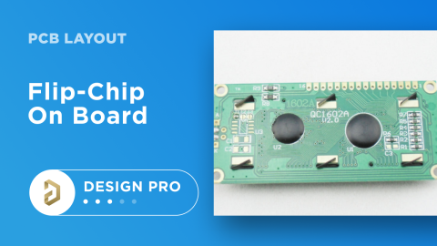
Small circuit boards like this power regulator can be designed with Altium Designer.
Other Tools for Small Circuit Board Design
There are other important features needed to design high-quality circuit boards, including small circuit boards and high-density designs. In addition to a standard set of ECAD features, designers need full control over their stackup, plane and polygon designs, and component orientation to ensure everything can be fit onto a small PCB. Once designs need to be evaluated, everything in the PCB layout needs to be quickly checked to ensure manufacturability, and manufacturing documentation needs to be generated for fabrication and assembly.
Altium Designer includes all these features and many more in a single program. While other circuit board design platforms separate these important features into different applications, Altium Designer gives you access to everything you need in one application with a consistent workflow. Take your next PCB design from concept to finished product with Altium Designer.
The Power of Rules-Driven in Altium Designer
The rules-driven design engine in Altium Designer is the glue that allows every design feature to be integrated into a single program. The comprehensive toolset in Altium Designer checks all aspects of your schematics and layout against your PCB design rules as you create your design, which helps you catch errors early in the design process. This also helps you stay productive as you create your circuit board layout.
- The design interface in Altium Designer includes everything you need to design high-quality circuit boards of any shape and size.
Learn more about Altium Designer‘s integrated PCB design tools.
- Altium Designer’s routing features are ideal for a range of designs that require high-density routing on small circuit boards.
- Whether you’re creating a large or small circuit board, you can share your PCB design files, enclosure design data, and manufacturing documents with collaborators using the Altium 365 platform.
Learn more about sharing your PCB design data on Altium 365.

Complete schematic design, PCB layout, and component sourcing in Altium Designer.
Whether you need to design a very large or very small circuit board, you can use the complete set of CAD tools in Altium Designer to create high-quality PCB layouts and prepare your boards for manufacturing. Altium Designer’s circuit board design features give you everything you need to create cutting-edge technology and prepare your new designs for full-scale manufacturing.
Altium Designer on Altium 365 delivers unprecedented integration to the electronics industry until now relegated to the world of software development, allowing designers to work from home and reach unprecedented levels of efficiency.
We have only scratched the surface of what is possible to do with Altium Designer on Altium 365. You can check the product page for a more in-depth feature description or one of the On-Demand Webinars.

关于作者
Related Technical Documentation
相关资源
目录
从设计到发布,全程无阻碍
- 让评审始终关联到正确的版本
- 减少交接中的混乱和返工
- 更早发现采购与发布风险
- 可独立工作,按需共享
开始使用
Thank you, you are now subscribed to updates.


 沪公网安备 31010502006411号