


PCB Silkscreen Guidelines

At a Glance
PCB silkscreen helps ensure your board is easy to read and test, and it aids assembly by clearly indicating component locations.


Every PCB has silkscreen on the surface layer, and you’ll see a range of alphanumeric codes, numbers, markings, and logos on PCB silkscreen. What exactly does it all mean, and what specifically should you include in your silkscreen layer? All designs are different, but there are some common pieces of information that will appear in any silkscreen in order to aid assembly, testing, debug, and traceability.
Anatomy of Your PCB Silkscreen
The silkscreen layer of your PCB is defined and printed during fabrication, and it will be used during assembly to verify component placement and footprints. The graphics and text that appear in the silkscreen layer are usually printed with a permanent non-conductive epoxy ink. Every circuit board I have produced uses white silkscreen, but you may see circuit boards that have silkscreen in a different color. Silkscreen can be placed during fabrication using a UV liquid photo-imaging process, which is similar to that used for solder mask application. If you need very small linewidths, your fabricator may use an alternative process called “direct legend printing” with a different type of ink.
For designers, there is some information that will be required for any design in order to put it through assembly. There are some instances where solder mask and silkscreen might be removed; I’ve been asked to do this in some experimental RF boards, in which case we produce a detailed assembly drawing so there is no confusion as to where different components will go. Other important information will be used for traceability, indicating regulatory compliance, identifying the part number for your PCBA, and even simple things like indicating polarity.
What Should Go on PCB Silkscreen?
Here is some of the information that should be included in your PCB silkscreen:
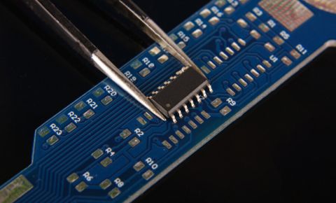
- A reference designator for each component
- Component values for passives
- A pin-1 indicator for ICs
- Polarity indicators for power/GND, or for polarity-dependent components (e.g., polarized capacitors and diodes)
- Component outlines where applicable
- Part numbers for the PCBA
- Company logos
- Manufacturer’s logo, serial number, and lot number
- Regulatory markings (see below)
- Connector pinouts, especially for pin headers
- Other notes regarding assembly, testing, installation, or operation of the PCBA
All of this information can get very cramped on a dense board; we’ll look at some ways you can organize your silkscreen markings later in this article. The example below shows an example PCBA containing some of the information in the above list.

Regulatory markings are used to indicate that the design has passed inspection or conforms to specific regulations. RoHS, FCC, CE, and the E-waste disposal markings are typically found on consumer and commercial products that have passed relevant inspection. Another marking that you might see on designs that have been inspected for safety is the UL marking. This marking indicates the design was fabricated and assembled by a UL-certified manufacturer according to the UL 796 and UL 94 standards.

Silkscreen in Components vs. Silkscreen in the PCB Layout
Inside your PCB design software, the silkscreen layer is defined in the top overlay layer (for the top layer silkscreen) or the bottom overlay layer (for the bottom layer silkscreen). All the silkscreen in your PCB will be placed in one of these two layers, either in the PCB layout directly or in your components. When I write “in the PCB layout,” I’m referring to any silkscreen that is placed in the PCB layout manually, meaning it was not placed automatically when components are imported into the designs.
Some PCB silkscreen markings should always be placed in a component footprint. The table below shows which of the pieces of silkscreen information should be placed in a component vs. placed manually in a PCB layout.
|
|
|
|
|
|
For UL, FCC, CE, or other markings, the easiest way to quickly place these is to create a component that only includes the relevant marking in the silkscreen layer. This way, you don’t need to manually import and place these from an image or a DXF file. To do this, simply create a new component and simply place only the imaging you need into an overlay layer in the PCB footprint; leave all other layers for the component empty. Read this article to see how to create a component and place silkscreen markings in Altium Designer.
How to Clean Up Silkscreen
When you’re working in a dense design, there is the possibility that your reference designators and other silkscreen markings overlap. This means you’ll likely have to clean up and rearrange some designators so that they do not overlap, are easy to read, and clearly indicate component positions. An example where this is needed is on groups of passives for decoupling or impedance matching, such as on the back side of a large BGA.
As an example, take a look at the image below. Here we have a very dense arrangement of capacitors on the backside of a BGA. Obviously, we can’t just leave every reference designator next to every component as it appears once imported into the board. Instead, these designators need to be spaced out so that they can all be read. However, this means that some designators will be moved farther away from the components.
In the silkscreen layer, the group of capacitors in the white boxes are arranged to match the placement and orientation of the nearby capacitors. I’ve drawn arrows to show which of the designators in the lower white box corresponds to different components. See if you can decode the same arrangement for the upper white box.

When your design is finished and you’re ready to export the design data, the top overlay layer in your Gerber files will contain all your silkscreen information. Don’t forget, if you’ve placed any silkscreen markings in the PCB as components, assign the “Standard (No BOM)” property to the component, or mark it as DNI/DNP in your BOM. This way, your assembler won’t wonder why you haven’t shipped this component to them when preparing for assembly.
Now you can use the best design tools to create and clean your PCB silkscreen with CircuitMaker, the easiest to use PCB design application. Users can also quickly create footprints for components and place required silkscreen markings. All CircuitMaker users also have access to a personal workspace on the Altium 365 platform, where they can upload and store design data in the cloud, and easily view projects via a web browser in a secure platform.
Start using CircuitMaker today and stay tuned for the new CircuitMaker Pro from Altium.

关于作者
Related Technical Documentation
相关资源
目录
从设计到发布,全程无阻碍
- 让评审始终关联到正确的版本
- 减少交接中的混乱和返工
- 更早发现采购与发布风险
- 可独立工作,按需共享
开始使用
Thank you, you are now subscribed to updates.


 沪公网安备 31010502006411号