Articles and resources related to PCB Components. Learn more about Component Creation and other relevant topics.
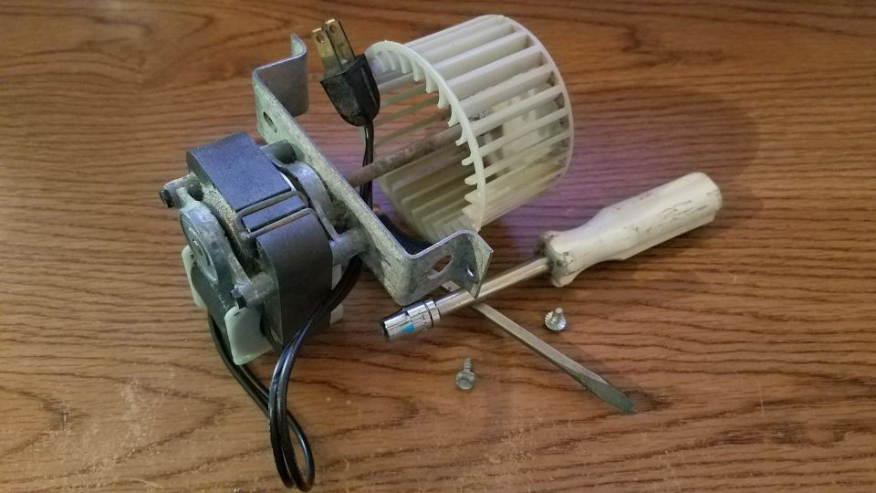
I’m in the middle of replacing the electric motor in my bathroom fan, but, unfortunately, I have no idea what
Growing up, I sometimes felt like an Army brat. My dad was in the Air Force, not the Army and
在布置印刷电路板时,务必要了解如何为设计元件创建封装。有些元件很常见,或者采用标准化封装,因此封装很容易找到。在某些情况下,封装生成可能需要您自己完成,并且您需要直接使用元件数据表中的信息。如果封装不正确,器件引脚可能与PCB焊盘无法对齐,或者器件可能违反间隙或间距规则,从而导致大量时间损失并产生额外成本。 设计您的PCB电路板时,您有时可以依靠已有的元件来为您的器件提供准确的封装。但是,情况并非总是如此,有时您总会不得不创建自己的封装。对于某些PCB设计软件包,这可能是一项艰巨的任务,在您精通之前需要经历难以接受的学习曲线。另一方面,借助Altium Designer®,您就可以使用强大的CAD工具快速生成元件封装。以下是如何使用Altium为设计元件创建封装的内容。 如何在Altium Designer中创建元件封装 通过以下4个步骤,在Altium Footprint Designer中生成元件封装: 创建焊盘 确定元件的高度和宽度 添加丝印层信息 保存封装 让我们逐步完成此过程,了解创建元件封装是多么简单。 通过4个简单步骤,在Altium Designer中创建封装设计,具体操作如下: 第1步:创建焊盘 您将需要元件的焊盘模式,可以在元件数据表的末尾或在您选择的数据库中找到。在本例中,让我们使用流行的PIC24FJ64GA004微控制器。该元件采用44引线塑料薄方型扁平式封装。 在Altium Footprint Designer中,位于文件
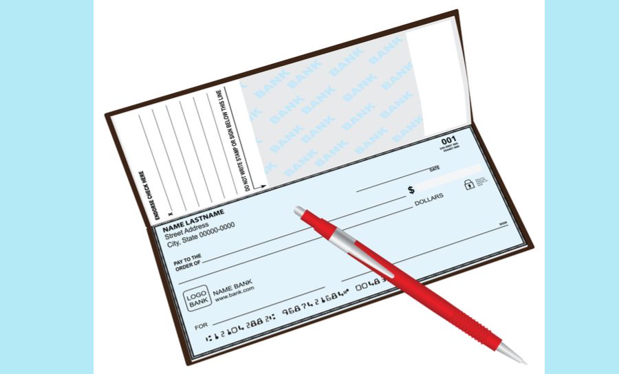
Some years back I was helping my son organize his finances, and he was explaining to me how he didn’t
My dog is so old that he sleeps 20 hours a day and naps the other four. Therefore it was
One of the dictionary definitions of the word “template” is; anything that determines or serves as a pattern or a
PCB design libraries need to be created and maintained by a design team. See how you can implement a PCB library creation process.