Skip to main content
Mobile menu
Altium Develop
资源 & 支持中心
Altium 365 免费工具
Gerber Compare
在线 PCB 查看器
了解产品
下载
联系我们
关注微信
扫描二维码
关注Altium微信平台
资源 & 支持中心
所有资源
支持中心
文档
官方直播
Altium 社群
社群
Bug提交
创意
教育
学生实验室
教育者中心
Altium 教育课程
Search Open
Search
Search Close
登录
Home
Main menu
首页
PCB设计
团队协作
元器件创建
PCB数据管理
PCB设计输出和文档
ECAD/MCAD
HDI设计
高速设计
多板设计
PCB布局
PCB布线
PCB供应链
电源完整性
RF设计
刚柔结合板PCB设计
原理图输入
信号完整性
PCB设计仿真/分析
软件
Develop
Discover
Agile
Altium的365
Altium Designer的
资源中心
项目
Altium Academy
工程新闻
指南书
新闻通讯
播客
项目
培训课程
网络研讨会
白皮书
Overview
All Content
CoDesign and CoEngineering (ECAD/MCAD Collaboration)
Component Management and Libraries
Data Management and Version Control
Manufacturing Outputs and Compliance
PCB Design and Layout
Supply Chain and Component Sourcing
Systems and Product Design
Filter
清除
Role
全部
ECAD 库管理员
电气工程师
工程经理
IT 经理
机械设计工程师
PCB 设计工程师
采购经理
软件工程师
Software
全部
开发
敏捷
Altium Designer
Altium 365
Assembly Assistant
BOM Portal
Cloud PLM Connector
PLM集成
GovCloud
Jira Integration
Octopart
Requirements Portal
Content Type
全部
指南
网络研讨会
视频
播客
白皮书
Region
全部
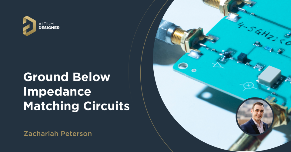
Should You Remove Ground Below Impedance Matching Networks?
9 min
Blog
电气工程师
Impedance matching networks in a PCB layout might need to have ground cleared from them. We’ll explore when to remove ground in this short guide.
阅读文章
New Opportunities for PCB Education with John Watson
3 min
Podcasts
John Watson talks about the importance of education for designers, what it's like working with students, and what new opportunities there are for PCB designers in today's market.
阅读文章
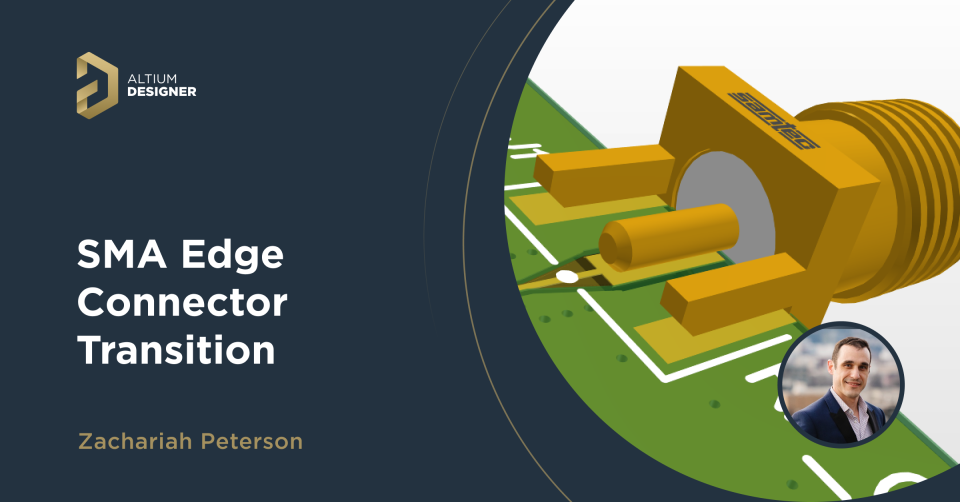
SMA Edge Connector Transitions in an RF PCB
6 min
Blog
SMA edge connector footprints sometimes require ground clearance below the connector’s coaxial pin. We’ll show why this can arise and how to qualify the need for ground clearance.
阅读文章
Beyond Schematics: PCB Process Engineer
9 min
Engineering News
Are you curious about what goes into creating the electronic devices we use every day? Do you want to know
阅读文章
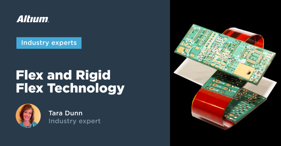
Flexible Circuits: Start with the Basics
5 min
Blog
There are several advantages to using flexible materials. Size, weight, the ability to bend around corners and to flex during use to name just a few. Read this blog to learn more!
阅读文章
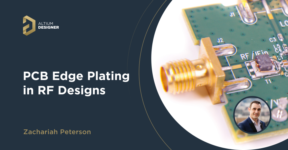
Guide to PCB Edge Plating in RF Design
5 min
Blog
RF designs sometimes use PCB edge plating to contain electromagnetic fields and ruggedize a PCBA.
阅读文章
IPC Focus on Substrates, Manufacturers Focus on Boards
6 min
Newsletters
March 24, 2023 ONTRACK BI-WEEKLY This edition of our newsletter focuses on current developments in electronics manufacturing, spanning from packaging
阅读文章
Pagination
First page
« First
Previous page
‹‹
Page
176
当前页面
177
Page
178
Page
179
Page
180
Page
181
Next page
››
Last page
Last »


 沪公网安备 31010502006411号