
Mobile menu
解决方案
Altium Develop
在 Altium Designer 中设计先进 PCB,可独立设计,也可在需要时连接评审、数据来源和发布协同。
Altium Agile Teams
在多学科电子开发与协作中引入结构化流程,确保效率与速度不受影响。
资源 & 支持中心
Altium 365 免费工具
Gerber Compare
在线 PCB 查看器
了解产品
下载
联系我们
关注微信
扫描二维码
关注Altium微信平台
资源 & 支持中心
用户指南
实战讲堂
学习中心
技术文档
支持中心
常见问题
Altium 社群
社群
Bug提交
创意
教育
学生实验室
Free access to professional PCB design software, training, and learning resources for students
教育者中心
A comprehensive education platform providing curriculum, software, training, and classroom resources for educators
Altium 教育课程
Free college- and university-level PCB design curriculum designed to prepare students for real-world engineering careers
Search Open
Search
Search Close
登录
设计库
Main menu
首页
PCB设计
团队协作
元器件创建
PCB数据管理
PCB设计输出和文档
ECAD/MCAD
HDI设计
高速设计
多板设计
PCB布局
PCB布线
PCB供应链
电源完整性
RF设计
刚柔结合板PCB设计
原理图输入
信号完整性
PCB设计仿真/分析
软件
Discover
Develop
敏捷团队
敏捷企业
Altium 365
Altium Designer
资源中心
项目
Altium Academy
工程新闻
指南书
新闻通讯
播客
项目
培训课程
网络研讨会
白皮书
首页
设计库
设计库
PCB设计库为您的设计团队改进efficency。浏览我们的资源库,详细了解库管理,可免费使用的PCB设计库。
Altium's Data Management Solutions
Solutions for ECAD Librarians
Documentation for File Based Libraries
Overview
指南
网络研讨会
视频
Tech Docs
All Content
Filter
found
Sort by
Most Recent
Most Popular
Title (A-Z)
Title (Z-A)
Role
ECAD 库管理员
电气工程师
工程经理
机械设计工程师
PCB 设计工程师
采购经理
软件工程师
Software
Altium Develop
Altium Agile 团队
Altium Agile Enterprise
Altium Designer
Altium 365
BOM Portal
Ciiva
PLM集成
MCAD CoDesigner
Octopart
Content Type
指南
视频
网络研讨会
白皮书
播客
Region
EMEA
Americas
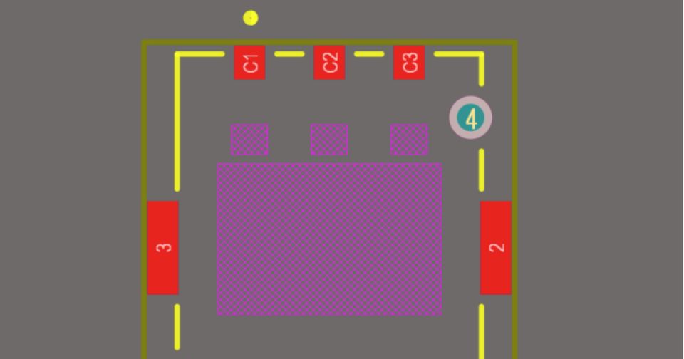
What's With All the Layers in PCB Footprints?
6 min
Blog
ECAD 库管理员
Your PCB footprints contain many layers. Which of these layers are most important and what should they contain? We’ll explore in this article.
阅读文章
Does Anyone Still Use DIP Components?
5 min
Blog
DIP components are less-often used in professional PCB design projects for new products, but legacy products may still need these parts.
阅读文章
您需要了解的有关保形涂层的所有信息
1 min
Blog
Manufacturing Engineers
Production Managers
与Mark Harris一起探索保形涂层的基础知识。保形涂层是一种应用于电子电路的保护层,可防止湿气和灰尘等环境因素的影响。
阅读文章
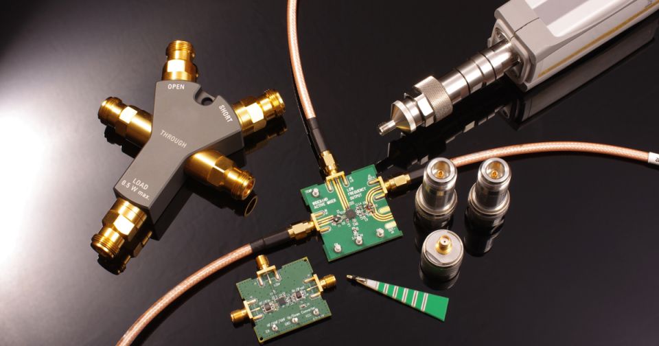
How to Design a Bias Tee for a Power Amplifier
11 min
Blog
Bias tees are used in some RF systems to separate AC and DC power along a particular line. Learn more about bias tee design in this article.
阅读文章
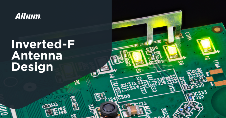
Inverted-F Antenna Design For a PCB
6 min
Blog
PCB 设计工程师
电气工程师
Learn how to design an inverted-F antenna for an RF PCB layout.
阅读文章
How to Design an IC Carrier PCB
6 min
Blog
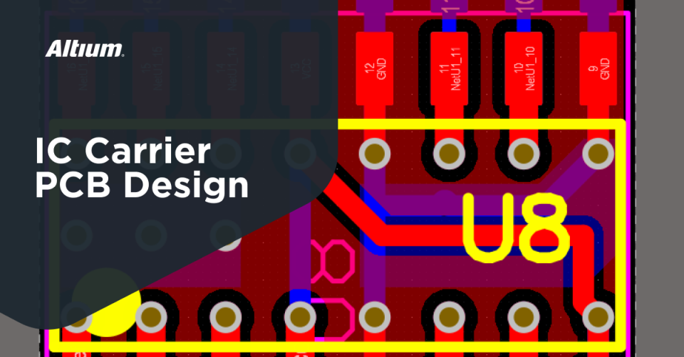
Carrier boards for integrated circuits can be used as interposers whenever there is an incorrect PCB land pattern.
阅读文章
PCB Design Rules for Chip-on-Board Layout
6 min
Blog
There is one simple type of packaging that is not really packaging in the conventional sense: chip-on-board.
阅读文章
Pagination
First page
« First
Previous page
‹‹
页面
5
当前页面
6
页面
7
页面
8
页面
9
页面
10
Next page
››
Last page
Last »