


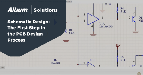


Quickly Replicate Circuits with a Connection Room in Your PCB Layout


Modern PCB designs can get very complex, and designers need tools to help them stay organized. Schematic sheets are a great start, but simply organizing different circuit blocks into different schematics is not enough to ensure your designs are organized. Altium Designer unifies your schematic design and PCB layout tasks into a single program, and it includes a PCB connection rooms feature to keep your circuit blocks synchronized. Here’s how you can best use the rooms feature in Altium Designer to keep your complex designs organized.
ALTIUM DESIGNER
The only PCB design package with powerful organization features built on a unified rules-driven design engine.
As you progress through the deep world of PCB design, your schematics and layouts will only get more complex. It’s hard to keep track of portions of a layout that require specific sets of design rules, and you still need to see the link between different sections of a PCB layout and schematics. Design tools that aid this type of synchronization make it easy to create, move, copy, and change groups of components as a single unit.
In Altium Designer, these blocks of components, traces, and other structures in a PCB layout are called PCB “component rooms,” or just rooms for short. Thanks to Altium Designer’s unified PCB design environment and interface, designers can create rooms on their own or generate them automatically as they work through their design. Here’s why you should take advantage of these features in your PCB design software and how Altium Designer makes these tasks easy.
What You Can Do With a PCB Connection Room
Whenever you need to move a large group of components, replicate multiple circuit blocks, or apply design rules to a set of components and layout features, you can use a room in Altium Designer. Rooms can be easily used to expedite data transfer from schematics and into a new PCB layout before you arrange components. The components in a room will be assigned a component class, which can then be used to set specific design rules for every layout feature and component in the room.
How to Quickly Create and Configure a Room in Your PCB Layout
Not all PCB design software platforms include tools needed to create a connection room for your PCB layout. The best PCB layout tools let you quickly create a connection room by selecting a group of components in your PCB layout and assigning a room name. Altium Designer makes this process easy with a powerful set of PCB layout features and CAD utilities. Once you’ve created your room in the PCB layout, you can start specifying design rules and locking components in place as you continue building your PCB layout.
- Whether or not you want to keep rooms in your PCB layout, you’ll need to ensure your layout follows basic and application-specific PCB design rules and guidelines.
Learn more about best practices and guidelines for PCB design.
- Not all design rules are relevant to your PCB, but you can ensure your board operates correctly when you apply the right PCB design rules to connection rooms.
Learn more about important design rules you can apply to your PCB layout.
- When you use Altium Designer, you can save portions of your design as snippets and once you’ve created a room and locked components as circuit blocks. This helps you stay organized and lets you quickly reuse portions of a design.
Learn more about setting up reusable blocks in Altium Designer.

Placing a group of elements into a room lets you apply design rules to very specific sections of a PCB layout.
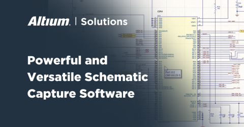
Organize Your Components With the Best Schematic Editor
Creating rooms from a completed PCB layout can be an important task to help you stay organized, but you can also enforce organization directly in your schematics. Doing this early in the design lets you build organization into your layout before you’ve ever arranged your components. You can plan out your design rules and constraints early, and it saves you time when working on complex designs.
Because Altium Designer lets you design schematics and layout a PCB in the same program, the two sets of data are automatically linked. Once you capture your schematics and import them into a new PCB layout, you’ll have the option to create a component room for each schematic sheet. The rooms that are created nicely reflect the organization you’ll enforce in your design, and you can still modify or create rooms in the layout as needed.
Instantly Create Rooms from Hierarchical Schematics
Altium Designer’s hierarchical schematic design features also integrate with the standard PCB layout editor. Just like when working with flat schematics, rooms can be instantly created from hierarchical schematics and applied to repeated circuit blocks within your hierarchy. You can then set design rules across connection rooms and component classes in your design.
- Complex designs can get very messy when working in a single schematic sheet, but there are some simple strategies you can use to organize circuits in your schematics.
Learn more about organizing messy schematics in Altium Designer.
- Hierarchical schematics are an alternative to a flat design architecture, where multiple circuit blocks are linked together at a high level.
Learn more about the difference between flat and hierarchical schematics.
- Altium Designer lets you make the transition from schematic to layout instantly while enforcing the organization you build into your schematics.
Learn more about creating a new PCB layout from your schematics in Altium Designer.

The hierarchical schematic design features keep your most complex designs organized, and you can quickly create component rooms from your schematic sheets.
Keep Your Designs Organized with Altium Designer
Altium Designer is more than a circuit diagram editor or PCB layout utility, it’s a unified rules-driven PCB design platform that helps you go from concept to product in a single program. You can enforce the design hierarchy and organization you need early in the design process, and you can access a complete set of PCB layout utilities as you create your layout. When you’re ready to prepare for production, all your design data and your project structure will be copied into your deliverables. All these features help you stay more productive and create higher quality products.
Altium Designer Helps You Stay at the Cutting Edge
The secret to Altium Designer’s powerful interface and organizational tools is its rules-driven design engine. The rules engine ensures your schematics and PCB layout remain synchronized, even when using connection rooms for your PCB layout. Every aspect of your circuit board layout can be inspected as you create your design, and custom design rules can be created for any application.
- Altium Designer’s rules-driven design engine automatically checks your PCB layout as it’s created. The online DRC engine lets you build custom design rules for your board and allows you to run DRCs anytime during design.
Learn more about the rules-driven design environment in Altium Designer.
- Complex designs like multiboard systems can be difficult to keep track of, but the schematic editor in Altium Designer makes these designs easy and accurate. Just like with hierarchical schematics, you can keep your multi-board designs organized with Altium Designer.
- After you’ve completed your design and you’ve performed all the necessary rule checks, you can instantly share your design data in the cloud using the Altium 365 platform.
Learn more about collaborative PCB design with the Altium 365 platform.

Altium Designer helps you stay organized by linking your schematics and PCB layout into a unified design environment.
Other design software forces you to create messy schematics and doesn’t help you stay organized. Altium Designer has changed PCB design workflows thanks to its unified design environment. You can keep yourself at the cutting edge and at your most productive with the powerful PCB design features in Altium Designer.
Altium Designer on Altium 365 delivers unprecedented integration to the electronics industry until now relegated to the world of software development, allowing designers to work from home and reach unprecedented levels of efficiency.
We have only scratched the surface of what is possible to do with Altium Designer on Altium 365. You can check the product page for a more in-depth feature description or one of the On-Demand Webinars.

关于作者
Related Technical Documentation
相关资源
目录
从设计到发布,全程无阻碍
- 让评审始终关联到正确的版本
- 减少交接中的混乱和返工
- 更早发现采购与发布风险
- 可独立工作,按需共享
开始使用
Thank you, you are now subscribed to updates.


 沪公网安备 31010502006411号