


How to Design a Microstrip to PCB Waveguide Transition

At a Glance
Here’s how you can design a microstrip to waveguide transition for your RF PCB layout.


RF structures can be complicated to design and layout, particularly because many RF systems lead double lives as digital systems. Getting an analog signal out of a component and into a waveguide for high isolation routing is not so simple as placing a microstrip or stripline coming off your source component. Instead, you need to create a special microstrip to waveguide transition structure to ensure strong coupling into and out of your waveguide.
These structures can be quite complicated, and empirical formulas describing their functions often need to be determined using field solvers, approximations, or measurements. Although they can be tough to design, they have some simple signal integrity rules that apply to other traces in your PCB. Once you understand these relationships between the microstrip feedline and your waveguide structure’s impedance, you’ll know exactly what to analyze in your field solver results for your waveguide structure.
A Microstrip to Waveguide Transition Determines Impedance
Like many high speed and high frequency design choices, the point of placing a microstrip to waveguide transition is to set the impedance of the waveguide to a desired value. More specifically, the goal is to set the input impedance looking into the waveguide so that it matches the microstrip’s impedance. This keeps return loss low at the interface between the microstrip and the waveguide.
Unfortunately, you often can’t simply connect a microstrip to every waveguide for a number of reasons. Consider a typical 50 Ohm microstrip on an 8-layer board (width 17 mils with Dk = 4.2). For a coplanar waveguide, the width required for 50 Ohms impedance on the same substrate is ~20 mils. But for a substrate integrated waveguide, the width required is very large (several mm). The transition structure matches the input impedance using a smooth transition between different widths. In this way, you keep reflections as low as possible throughout the waveguide’s bandwidth.
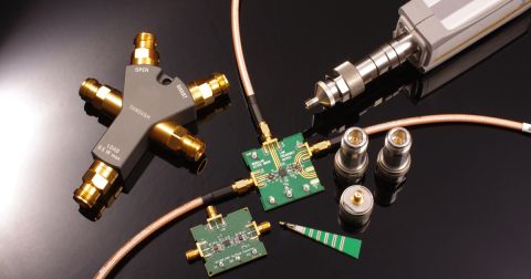
The exact type of structure you need depends on whether you’re transitioning into a waveguide on the printed circuit board or an external waveguide through a flange. We’ve done both of these on a single interconnect to route a high frequency signal through a noisy environment. Let’s look at some options for printed circuits first:
Printed Waveguides on a PCB
The transition into a waveguide on a PCB can be performed with a few different structures:
- Tapered transition. This is probably the most common structure used to transition from microstrips to coplanar waveguides, substrate integrated waveguides, and mode-selective transmission lines. These transitions are broadband; they permit a broad range of frequencies to transmit into the edge of the waveguide. Learn more about taper design here.
- Stepped transition. This is also common as it is easy for anyone to design the series of stepped patches leading from the microstrip to the waveguide. These intermediate patches are just at the edge of being electrically short and are best for lower frequencies.

Once the signal enters the waveguide, what happens next depends on whether the signal excites one of the cavity modes in the waveguide. Take a look at this recent article to see how different modes can be designed and excited in a waveguide.
Waveguides Through a Flange
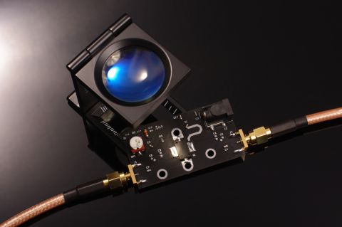
This involves placing an antenna at your waveguide flange on your PCB. I’ve done this by placing a slot antenna on the wall of the waveguide, but this can also be done with a simple radiating microstrip. No matter how you create your radiating element, the goal is to launch a propagating wave through the aperture in the flange without reflection. This is also a matter of matching the input impedance of the waveguide flange to the impedance of the radiating microstrip antenna.
An example with a patch antenna is shown in the graphic below. In this example, the waveguide short pattern region modifies the directionality of emission from the open microstrip line. The matching element is a floating conductor that modifies the input impedance of the waveguide to match that of the microstrip. Finally, the via fence around the waveguide opening acts as an extension of the flange around the radiating element to provide isolation.

Normally, when using a flange for an external waveguide, you would not typically use a floating patch to match the flange input impedance to the microstrip impedance. Instead, you would place an iris in the cross-section of the flange to match its input impedance. This is like putting a parallel LC network in parallel with the waveguide impedance. Most waveguide manufacturers already do this for you, so you won’t need to worry about custom flange design if it’s not your area of expertise.

Placing a Microstrip Transition in Your PCB Layout
These transition structures can be difficult to design, and designers will often rely on a field solver utility to determine the right structural parameters. Once the geometry for your microstrip to waveguide transition has been determined, you can easily place a transition structure using the CAD tools in your PCB layout software.
I prefer to do this with polygon pour on the relevant layer, and then I place pads on the input and output ports. This allows the microstrip section to be quickly routed onto the transition structure, and then the transition structure can be connected to the waveguide section. Add in some schematic symbols, and you’ve got a simple way to add the structure into your schematics before you create your PCB layout. Take a look at this article for a more thorough guide for substrate integrated waveguides.

Since this type of structure will normally be used in an RF PCB, it is recommended to have the soldermask removed from the taper regoin and the two connected interconnects. The reason for this is the loss tangent in the solder mask, which will have a loss tangent that is comparable to the value seen in standard FR4 laminate. Removing the solder mask will remove that additional loss and will extend the useful propagation distance for microwave signals.
The complete set of CAD tools in Altium are ideal for creating a microstrip to waveguide transition, patch antennas, or other unique printed RF structures in your PCB. When you’ve finished your design, and it’s time to share your work with your collaborators, you can use Altium to share and manage your design data.

关于作者
Related Technical Documentation
相关资源
目录
从设计到发布,全程无阻碍
- 让评审始终关联到正确的版本
- 减少交接中的混乱和返工
- 更早发现采购与发布风险
- 可独立工作,按需共享
开始使用
Thank you, you are now subscribed to updates.


 沪公网安备 31010502006411号