


PCB First-Pass Yield: Small Decisions That Make a Big Difference

At a Glance
Designing for first-pass yield means fewer delays, lower costs, and better boards. Learn the layout choices that help you get it right the first time.


If you've ever been on the receiving end of a circuit board that failed during first-pass assembly, you know how frustrating it can be. The board looks good, the design checks out electrically, but something goes wrong during fabrication or assembly, and the result is a costly delay. When it comes to designing PCBs, especially in advanced applications like Ultra HDI or flex, getting it right the first time isn’t just about pride, it is about performance, yield, and cost.
Let’s take a closer look at the subtle design choices that can make a big impact on first-pass yield, and what you can do to avoid surprises on the production floor.
Why First-Pass Yield Matters
First-pass yield is exactly what it sounds like: the percentage of boards that pass inspection and testing the first time through the manufacturing process, with no rework required. High first-pass yield translates directly into higher efficiency, lower costs, and happier customers. It also builds trust with your manufacturing partners, when they know your designs are production-friendly, they’re more likely to push your jobs through faster and with fewer concerns.
Design Rule Check: Your First Line of Defense
Altium tools will flag major design rule violations. But when you’re pushing fine features, staggered microvias, or unconventional stack-ups, it may be better to collaborate with your fabrication partner to load process-specific design rules into your tools. What’s manufacturable in one shop may not be in another.
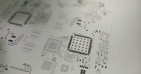
Check your minimum trace widths, spacing, annular ring requirements, and drill-to-copper clearances. For Ultra HDI designs, don’t assume your standard 3 mil spacing applies. For flex circuits, layer transitions and coverlay openings need to be dialed in with precision.
Pay Attention to Component Footprints
Incorrect or overly tight footprints are a leading cause of first-pass failures. Ensure that your component library reflects actual package sizes, solder paste requirements, and land patterns recommended by the manufacturer. If your footprints are too aggressive, you'll get bridging, tombstoning, or opens. If they’re too conservative, you might sacrifice valuable space or compromise performance.
Be especially careful with BGAs, fine-pitch connectors, and components placed near board edges. And always consider how thermal reliefs and copper balancing will affect solder flow.
Optimize for Soldering Success
First-pass yield and soldering go hand-in-hand. Avoid component orientations that force the pick-and-place machine to rotate unnecessarily, as misalignment increases the risk of placement errors.
For double-sided assemblies, be mindful of component mass on the bottom side during reflow; heavy parts can shift or fall if they’re not anchored correctly. And review your solder mask strategy: tenting vias, for example, can prevent solder from flowing where it shouldn't.
Use solder paste apertures that match your manufacturing partner’s stencil design guidelines. In Ultra HDI boards, where spacing is tight, slight over- or under-deposition of paste can make or break your yield.
Include Fiducials, Tooling Holes, and Board-Level Features
First-pass success starts before the solder goes down. Global and local fiducials help automated equipment align accurately. Tooling holes ensure consistent board handling and support. If you're using edge connectors or test points, make sure they’re clearly defined and accessible.
Missing or inconsistent board-level features can create chaos on the line, even if the rest of the design is flawless.
Don’t Overlook the Stack-Up
Layer alignment, via structures, and copper balancing all influence your first-pass success. If you’re using sequential lamination, call that out clearly in your documentation. Unbalanced stack-ups can lead to warpage or delamination, especially in rigid-flex designs.
For Ultra HDI, stacked vias, thin dielectrics, and ultra-fine traces leave very little room for error. Your stack-up should include realistic tolerances, clear materials, and process notes.
Use Realistic Test Points and DFT Guidelines
Design for Test (DFT) should be part of your layout process from day one. If you leave it until the end, you risk poor coverage or boards that are difficult (or impossible) to test.
Add sufficient test access for key nets, including power and ground. For high-speed or sensitive circuits, consider using boundary scan or built-in self-test (BIST) structures. Label and locate test points with inspection and accessibility in mind.
Involve Your Manufacturing Partner Early
This is one of the best ways to improve first-pass yield. Even the best design can fail in production if it wasn’t reviewed from a fabrication and assembly perspective. Share your design early, even in draft form, and ask for a DFM review.
Manufacturers can identify issues that don’t show up in your EDA tool - like soldermask misalignment, via-to-pad concerns, or silkscreen collisions. That feedback can help you make simple changes now that prevent costly fixes later.
Final Thoughts
Designing for first-pass yield is all about attention to detail. The small decisions you make, things like component spacing, solder mask design, test access, material selection, add up quickly. Get them right, and your board flows through the shop with minimal issues. Get them wrong, and you’re in for delays, added cost, and a lot of back-and-forth.
Start early. Ask questions. Partner with your manufacturer. Because when you aim for first-pass success, everyone wins.
关于作者
Related Technical Documentation
相关资源
目录
- Why First-Pass Yield Matters
- Design Rule Check: Your First Line of Defense
- Pay Attention to Component Footprints
- Optimize for Soldering Success
- Include Fiducials, Tooling Holes, and Board-Level Features
- Don’t Overlook the Stack-Up
- Use Realistic Test Points and DFT Guidelines
- Involve Your Manufacturing Partner Early
- Final Thoughts
从设计到发布,全程无阻碍
- 让评审始终关联到正确的版本
- 减少交接中的混乱和返工
- 更早发现采购与发布风险
- 可独立工作,按需共享
开始使用
Thank you, you are now subscribed to updates.

 沪公网安备 31010502006411号