Equip engineers with everything needed to design modern, high-performance PCBs.
Combine advanced PCB design with cloud-based collaboration to streamline development.
阅读来自业界的权威专家的最新信息PCB设计。
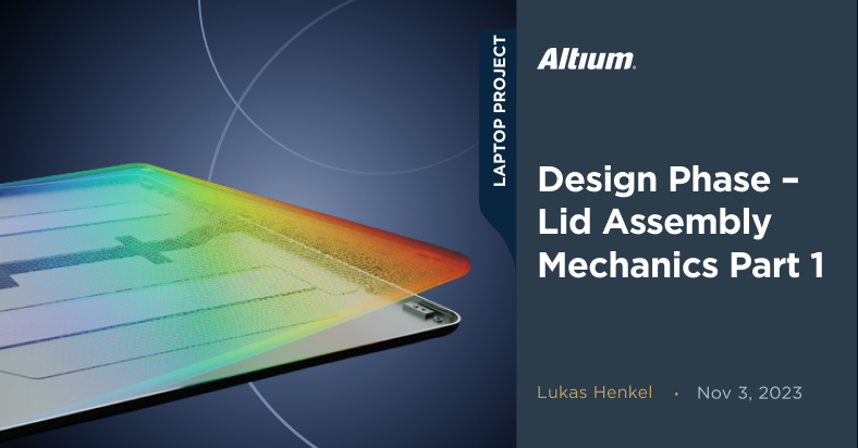
Welcome back to the open-source laptop project series! In the previous update, we discussed how to integrate the various sensors
Listen to the latest episode of OnTrack to hear a round up of the key PCB design trends from 2023. Explore themes such as evolving manufacturing dynamics, including shifts closer to the United States and Europe, influencing future innovations. Dive into the world of packaging design advancements and emerging trends such as robotic vision and new tools shaping the future of PCB design and the broader electronics market.
硬挠性PCB为高层次多板组件提供了一种替代方案。
Unlock the power of harness design with Altium's Michał Topolski! Explore the synergy of multi-board and harness design, experience hands-on insights, and discover seamless integration with Altium Designer for efficient workflows and user-driven improvements.
Explore the transformative world of 3D MID design in the OnTrack Podcast as Altium's Jack Henriques and Harting's Michael Mross discuss Altium's cutting-edge 3D routing tool. Gain insights into the vast potential of molded interconnect devices (MIDs) across industries and stay updated on the future of PCB design.
如果您的PCB外壳陷阱热量,您的电路板将开始过热。看看您如何设计一个有助于释放多余热量的外壳。
如果您自己制作PCB面板,有两种简单的方法可以分离PCBA。这些方法是鼠咬和V槽。以下是如何将这些设计到PCB面板中。