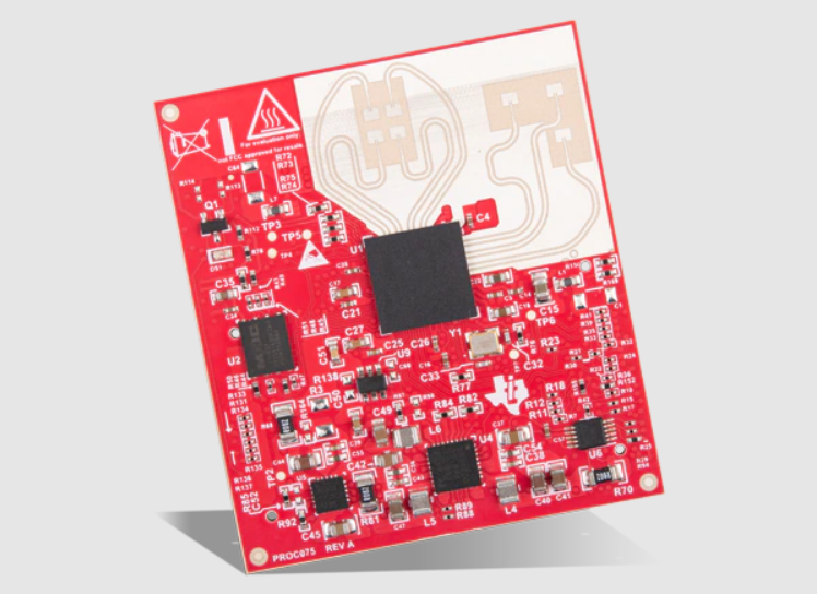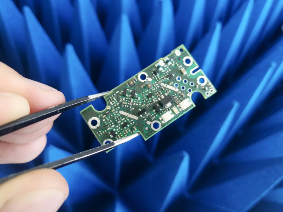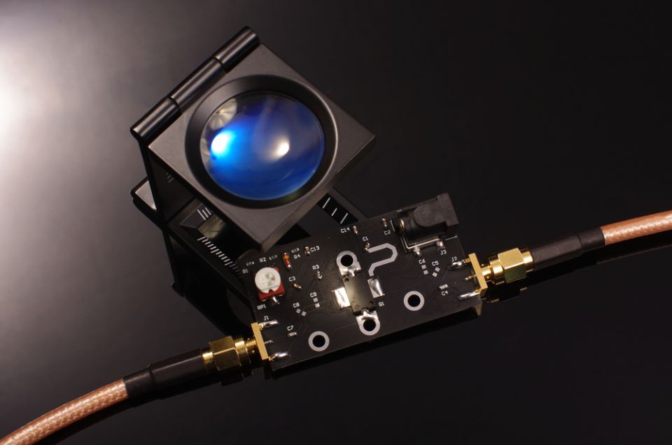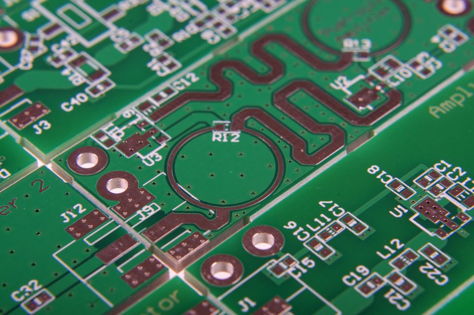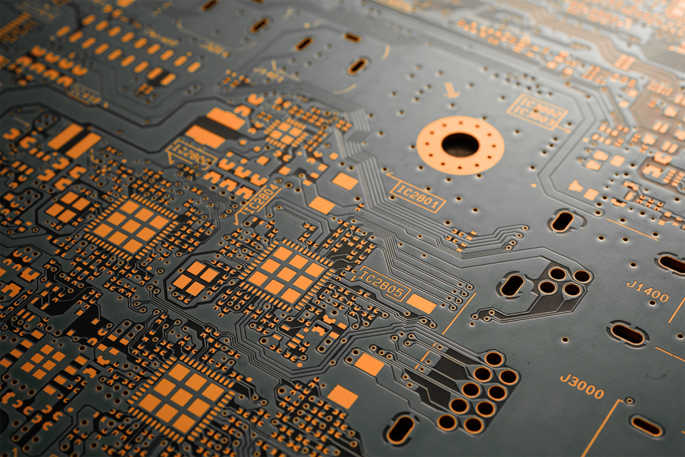
射频(RF)设计在高频下运行,因此需要精密的布局和布线以防止出现信号完整性问题。 RF PCB布局有时可能还包含带有数字元件的线段,精密的布局有助于防止RF和数字信号之间发生干扰。浏览我们的资源库,了解有关RF PCB设计、布局、布线和信号完整性的更多信息。
If you need alternative PTFE-based materials or low-Dk glass cloth materials, consider using a hybrid PCB stackup. You’ll have lower costs and the advantage of a low-loss material on one layer.
Here’s a comparison of the best RF PCB materials or your high-frequency analog products.
Read our guide to learn some of the best RF PCB design guidelines for layout and routing. We’ll also look at how simulation tools can help you evaluate your RF PCB layout.
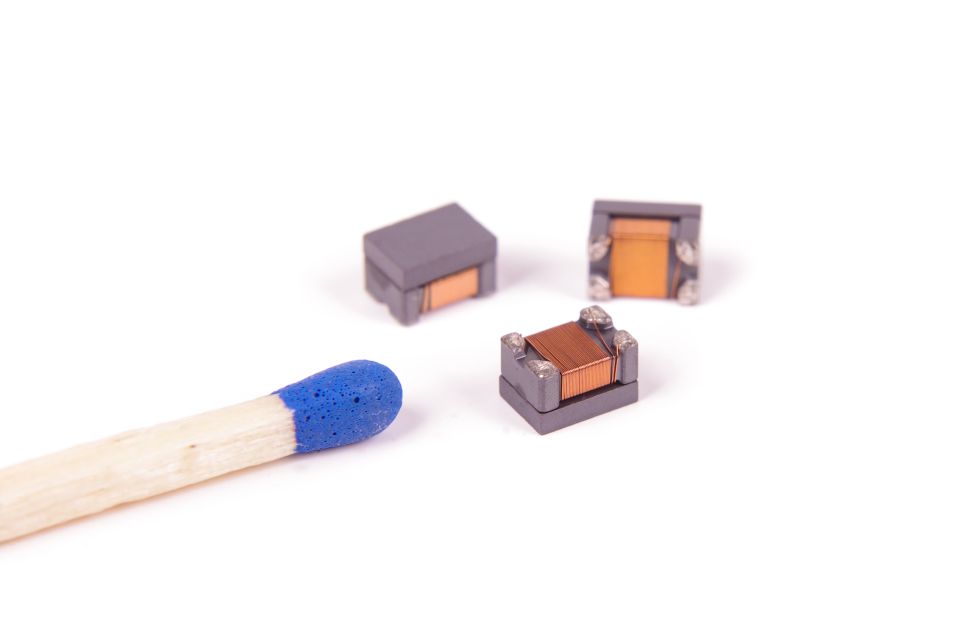
您是否想知道什么是平衡不平衡变压器(balun)?了解更多信息,并查看它如何适配您的射频PCB布局。
Here’s how you can design a microstrip to waveguide transition for your RF PCB layout.
Antipads in your PCB can create a signal integrity problem if not used properly. Here are some guidelines to help you get started.