Articles and resources related to 3D-MID and 3D PCB Layout & Routing. Check out Altium.com to learn more about PCB Layout and other relevant topics.
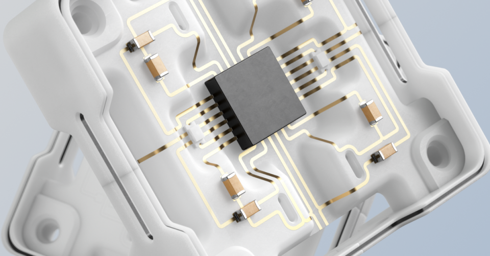
当产品外壳本身变成电路板时,设计规则就会彻底改变。结构电子基于 3D molded interconnect devices(3D-MIDs)等技术,将导电走线直接嵌入模塑塑料外壳中,消除了电气世界与机械世界之间的分隔。 这种集成正是关键所在。它能够实现更小的占用空间、更好的热管理以及原生 EMI 屏蔽。但这也意味着,一次机械几何形状上的变更,就可能破坏一条电气走线。这再次说明,电气工程师与机械工程师需要围绕创新设计开展协作,并在整个过程中进行实时数据共享。 关键要点 结构电子将外壳与电路板合二为一,把导电走线直接嵌入模塑塑料外壳中,从而实现更小的占用空间、更好的热管理以及原生 EMI 屏蔽。 一次机械改动就可能破坏电气设计。结构基板取代了标准 PCB 材料,在散热、信号完整性和屏蔽耐久性方面带来了新的权衡,电气工程师和机械工程师都必须加以考虑。 元器件和封装选择必须适应 3D 制造约束。Z 轴限制、模塑过程中极端的高温高压,以及表面曲率,都会限制哪些 IC
Peek inside breakthrough smart and AR glasses to find microdisplays, waveguides, IMUs, depth sensors, PMICs, graphite cooling, and compact connectivity.
Wearable electronics decoded: key breakthroughs, power solutions, and trends driving smarter, safer, always-connected devices across industries.
Discover how structural electronics merge circuits with materials to enable 3D, flexible, and wearable designs across aerospace, medical, and consumer tech.
Explore how structural electronics merges form and function, enabling lighter, smarter designs that redefine the future of electrical engineering.
Discover how electrical engineers use In-Mold Electronics (IME) to embed circuits into 3D surfaces, enabling sleek, durable, and space-saving smart interfaces.
What is Printed Electronics? Printed electronics is a rapidly evolving field that enables the creation of electronic circuits and components