Generate accurate manufacturing outputs while ensuring compliance with industry regulations, reducing production errors and time-to-market.
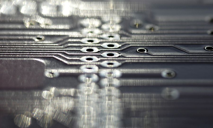
HDI PCBs with fine-pitch BGAs often use laser-drilled via-in-pad or microvia in-pad for BGA fanout routing. Here is how to design microvia-in-pad.
It’s to reuse items related to our work. Chefs reuse recipes, seamstresses reuse patterns, and engineers reuse circuitry. The problem
Having a wizard do your bidding is great when convoluted tasks need some hocus pocus. Removing tortuous steps to get
Via-in-pad and sub-lamination builds requiring etch control will limit allowed clearances in a PCB layout. Specifying a wrap plating process can help.
.
Easy PCB Drawings With Draftsman® Webinar Blog: 8/21/18 In case you missed our webinar on creating PCB drawings with Draftsman
“Picture if you will,” “Imagine a world where,” and “Submitted for your approval” are all quotes from Rod Serling, the