Skip to main content
Mobile menu
解决方案
Altium Develop
在 Altium Designer 中设计先进 PCB,可独立设计,也可在需要时连接评审、数据来源和发布协同。
Altium Agile Teams
在多学科电子开发与协作中引入结构化流程,确保效率与速度不受影响。
资源 & 支持中心
Altium 365 免费工具
Gerber Compare
在线 PCB 查看器
了解产品
在线商城
下载
联系我们
关注微信
扫描二维码
关注Altium微信平台
资源 & 支持中心
用户指南
实战讲堂
学习中心
技术文档
支持中心
常见问题
Altium 社群
社群
Bug提交
创意
教育
学生实验室
Free access to professional PCB design software, training, and learning resources for students
教育者中心
A comprehensive education platform providing curriculum, software, training, and classroom resources for educators
Altium 教育课程
Free college- and university-level PCB design curriculum designed to prepare students for real-world engineering careers
Search Open
Search
Search Close
登录
精神领袖
Main menu
首页
PCB设计
团队协作
元器件创建
PCB数据管理
PCB设计输出和文档
ECAD/MCAD
HDI设计
高速设计
多板设计
PCB布局
PCB布线
PCB供应链
电源完整性
RF设计
刚柔结合板PCB设计
原理图输入
信号完整性
PCB设计仿真/分析
软件
Discover
Develop
敏捷团队
敏捷企业
Altium 365
Altium Designer
资源中心
项目
Altium Academy
工程新闻
指南书
新闻通讯
播客
项目
培训课程
网络研讨会
白皮书
首页
精神领袖
精神领袖
Altium的与业界领先的专家紧密合作,在PCB的设计为您带来这些思想领导力资源。
Explore Altium Develop
Explore Altium Agile
Overview
指南
All Content
Filter
found
Sort by
Select
Most Recent
Most Popular
Title (A-Z)
Title (Z-A)
Role
电气工程师
工程经理
IT 经理
机械设计工程师
PCB 设计工程师
采购经理
Software
Altium Develop
Altium Agile 团队
Altium Agile Enterprise
Altium Designer
Altium 365
Ciiva
PLM集成
GovCloud
MCAD CoDesigner
Octopart
Content Type
指南
播客
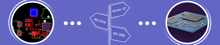
The Top Two File Format Alternatives to Replace Gerber RS-274X
3 min
Thought Leadership
Despite its popular use in about 90% of all PCBs designed worldwide, Gerber RS-274X has several practical limitations that can
阅读文章
The Biggest PCB Manufacturing Trends We’ve Seen This Year
4 min
Thought Leadership
The field of new technology in PCB manufacturing is constantly evolving. Technology is improving, new innovations are being made, and
阅读文章
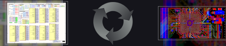
Automating PCB Design Environments: How to Simplify and Automate Your PCB ECO Workflow
2 min
Thought Leadership
Shuffling different programs for your schematic and PCB layout design changes costs both time and money. Altium Designer
®
tackles this
阅读文章
Really Bad PCB Design Advice to Not Follow
5 min
Thought Leadership
At Altium Designer, we’ve been in the PCB design software business for over 30 years. In that time, we’ve seen
阅读文章
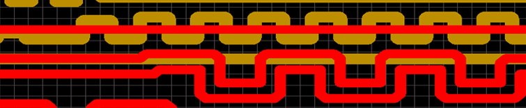
如何自动化您的高速设计流程
1 min
Thought Leadership
在电子表格中跟踪每个网段的长度、通孔深度或引脚长度可能是一项繁重的任务。了解如何通过Altium Designer
®
中的新技术自动化您的高速设计流程。 高速设计是电气工程师可以承担的最具挑战性的任务之一。许多因素可能影响高速信号的响应方式。一个误解是高速设计是系统时钟频率的功能。事实并非如此。实际上,高速是由上升时间、PCB堆叠中的阻抗控制、走线宽度和终端决定的。 更快的切换速度对工程师和PCB设计师来说基本上意味着两件事: 信号完整性问题 反射、串扰等。 通过控制阻抗布线、终端和PCB堆叠来实现信号完整性目标。 时序约束 确保多个信号几乎同时到达它们的目的地引脚 匹配信号路径的路由长度 高速设计的旧方法 在过去,工程师们不得不通过在电子表格中跟踪所有内容来处理信号完整性和时间约束问题。这使他们能够跟踪每个网络的每个单独段长、通孔深度、电阻长度和引脚长度。将每个网络的所有这些相加,然后在需要的地方添加信号长度,这使他们能够使组中所有网络的长度相等。这是一种过时的长度匹配方法,既繁琐又耗时。 如果你能自动定位相关设计规则,如长度和匹配长度,而不必浪费时间在电子表格中跟踪数据呢? 下载我们的免费高速设计和xSignals
®
白皮书,学习如何自动化你的高速设计流程。
阅读文章
Electronification of the World, One Wearable at a Time
4 min
Thought Leadership
As the world of electronic manufacturing shifts into the eras of Industry 4.0, IoT, and Big Data, it’s becoming more
阅读文章
Is IPC-2152 Holding Your Power Integrity Back?
2 min
Thought Leadership
For most designers, the Power Distribution Network (PDN) is a foreign and intimidating part of the PCB design process. But
阅读文章
Pagination
First page
« First
Previous page
‹‹
页面
112
当前页面
113
页面
114
页面
115
页面
116
页面
117
Next page
››
Last page
Last »










 沪公网安备 31010502006411号