Mobile menu
Altium Develop
资源 & 支持中心
Altium 365 免费工具
Gerber Compare
在线 PCB 查看器
了解产品
下载
联系我们
关注微信
扫描二维码
关注Altium微信平台
资源 & 支持中心
用户指南
实战讲堂
学习中心
技术文档
持中心
Altium Develop 常见问题集
Altium 社群
社群
Bug提交
创意
教育
学生实验室
Free access to professional PCB design software, training, and learning resources for students
教育者中心
A comprehensive education platform providing curriculum, software, training, and classroom resources for educators
Altium 教育课程
Free college- and university-level PCB design curriculum designed to prepare students for real-world engineering careers
Search Open
Search
Search Close
登录
制造和组装
Main menu
首页
PCB设计
团队协作
元器件创建
PCB数据管理
PCB设计输出和文档
ECAD/MCAD
HDI设计
高速设计
多板设计
PCB布局
PCB布线
PCB供应链
电源完整性
RF设计
刚柔结合板PCB设计
原理图输入
信号完整性
PCB设计仿真/分析
软件
Develop
Discover
Agile
Altium的365
Altium Designer的
资源中心
项目
Altium Academy
工程新闻
指南书
新闻通讯
播客
项目
培训课程
网络研讨会
白皮书
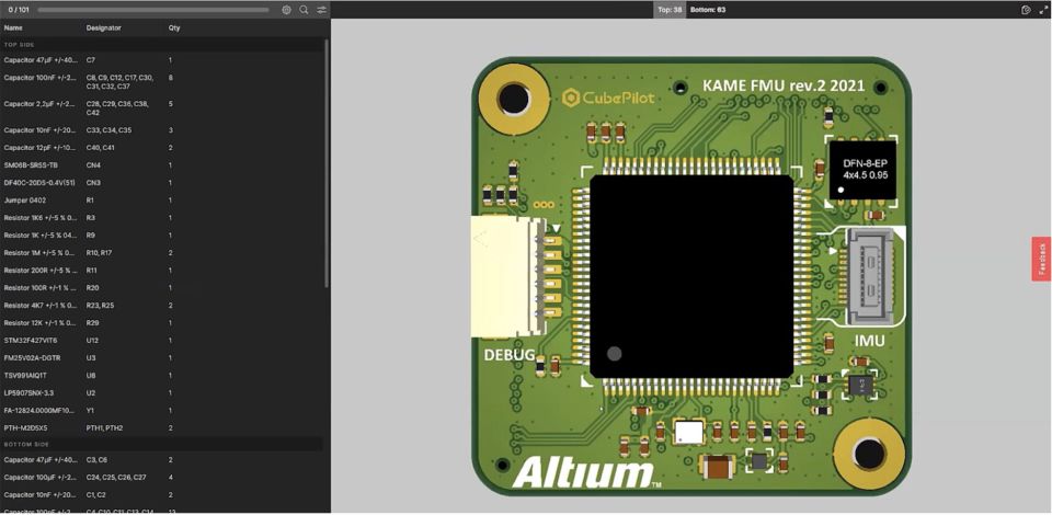
Manual Board Assembly
Build boards efficiently with intuitive guidance.
Learn More
首页
制造和组装
制造和组装
浏览我们的资源库了解更多关于PCB设计和电路板制造和组装。
Altium's PCB Assembly Solutions
Onboarding Guide for Assembly Assistant
Assembly Assistant Documentation
Overview
指南
网络研讨会
Tech Docs
All Content
Filter
found
Sort by
Most Recent
Most Popular
Title (A-Z)
Title (Z-A)
Role
电气工程师
机械设计工程师
PCB 设计工程师
采购经理
Software
开发
敏捷
Altium Designer
Altium 365
Assembly Assistant
BOM Portal
Octopart
Content Type
指南
网络研讨会
播客
Ultra HDI: It’s Not Just Buzzword
5 min
Blog
PCB 设计工程师
Systems Engineers/Architects
Manufacturing Engineers
Ultra HDI pushes PCB design beyond traditional HDI, enabling higher density, miniaturization, and performance. Learn how it’s shaping next-gen electronics.
阅读文章
DFM/DFA Requirements in Systems Engineering
10 min
Blog
PCB 设计工程师
Manufacturing Engineers
Ensure manufacturable, cost-effective PCB designs with DFM/DFA best practices. Learn how to integrate CAD, CAM, and key requirements for seamless fabrication.
阅读文章
Backdrill-and-Fill For Blind and Buried Vias in PCBs
10 min
Blog
PCB 设计工程师
Blind vias aren’t just for HDI PCBs, they are also used in standard builds with mechanical drilling and no thin
阅读文章
How to Speed Up Your Manual Assembly Process with Assembly Assistant? The Story of XVP Photonics
11 min
Blog
Production Managers
Manufacturing Engineers
PCB 设计工程师
Learn how XVP Photonics boosted component placement accuracy and sped up manual assembly by 25% using Assembly Assistant. Discover their success story!
阅读文章
How PCB Designers Can Be Good Customers: A Fabrication Perspective
5 min
Blog
PCB 设计工程师
电气工程师
A strong partnership with your fabrication services company can mean the difference between a smooth production process and costly delays
阅读文章
Direct Metallization Process for PCB Via Fabrication
6 min
Blog
When vias and plated through-holes are fabricated in a PCB, they require a metal deposition and plating process in order
阅读文章
Should You Manufacture Your First PCB Prototype Locally?
6 min
Blog
电气工程师
PCB 设计工程师
Discover how to protect your intellectual property (IP) when creating PCB prototypes. Learn the pros and cons of local vs. global PCB manufacturing, and get valuable tips on data dissemination protocols to safeguard your design outputs. Make informed decisions to keep your product's IP secure while managing costs effectively.
阅读文章
Pagination
First page
« First
Previous page
‹‹
页面
1
页面
2
当前页面
3
页面
4
页面
5
页面
6
Next page
››
Last page
Last »