Addressing Forward and Backward Crosstalk in PCB Design

At a Glance
Crosstalk in high-speed PCB design appears FEXT and NEXT, and it depends on the rise time of signals traveling on transmission lines.


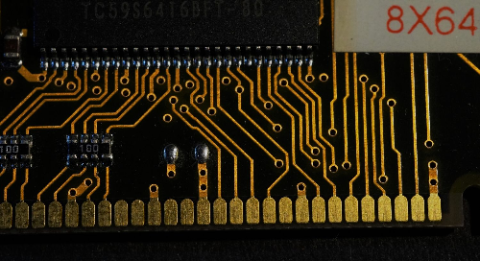
Crosstalk always occurs between electrical interconnects, both in PCBs, ICs, and any other system where the electromagnetic field interacts with two conductors. In a PCB, we typically refer to two types of crosstalk: forward and backward. These types of crosstalk originate from two coupling mechanisms: inductive and capacitive coupling. Some simple calculations are used to determine the amount of crosstalk between two transmission lines, and the amount of crosstalk in each line needs to be
Crosstalk Starts With Capacitive and Inductive Coupling
All crosstalk arises through two coupling mechanisms: capacitive and inductive coupling, which are mediated by mutual capacitance and mutual inductance, respectively. There will always be mutual capacitance and inductance between two traces on a PCB, although this generally applies to any pair of conductors. Both effects are present simultaneously, and the voltage/current pulse created in a victim trace from an aggressor trace depends on the combination of inductive and capacitive coupling.
To see how these parasitics arise, take a look at the diagram below. The two traces shown below have a characteristic impedance value and are connected to loads modeled as resistors. The mutual capacitance between the two traces arises due to the edge-to-edge proximity of the traces when routed in parallel. The traces also have their self-inductance (LP), but when the traces are routed in parallel these self-inductances have a mutual inductance between them.

It is the combination of the voltages and currents generated through these mutual capacitance and inductance values that will determine the amount of crosstalk. Both effects combine to produce crosstalk in two directions:
- Far-end crosstalk (FEXT), or forward crosstalk: propagates in the same direction as the aggressor signal
- Near-end crosstalk (NEXT), or backward crosstalk: propagates in the opposite direction as the aggressor signal
FEXT travels towards the receiver end of the victim line, and backward towards the driver end of the victim line.
Forward and Backward Crosstalk (FEXT and NEXT)
The amount of FEXT and NEXT are defined using two simple formulas. Consider we have two transmission lines on a PCB that have the same geometry, so they have the same self-inductance and self-capacitance. The velocity of the signal on each line is known and the traces are routed side-by-side over some specified length. The NEXT and FEXT coefficients (defining the ratio of aggressor and victim signals) are defined as:

Note that NEXT is limited to some upper limit value based on the fraction in the red box. FEXT can continuously increase along the length of the route, so very long parallel sections in a PCB will produce more FEXT.
FEXT and NEXT on a victim interconnect can be visualized in the time domain, as shown in the example below. As mentioned above, both occur simultaneously, and we can pick out the various contributions by looking at the two curves overlaid on each other. In the example below, NEXT is marked in red and it begins being measurable at the driver end right at time t = 0 (when the aggressor signal starts rising). FEXT is measured at the receiver end sometime later, in this case at t = 0.4 ns; this is because the FEXT pulse requires approximately 0.4 ns to travel to the receiver end of the circuit.

Note that there are additional pulses after the initial NEXT and FEXT measurements (at about 0.8 ns for NEXT and 1.2 ns for FEXT). These correspond to reflections from the opposite end of the interconnect, which then travel back to the measurement point. So for example:
- The initial NEXT pulse received on the victim appears at the driver's side at t = 0 ns
- The NEXT pulse reflects from the driver side and travels to the receiver side in t = 0.4 ns; some of that power at high frequencies reflects from the load capacitance
- The newly reflected NEXT pulse travels again back to the driver side throughout t = 0.4 ns; thus at t = 0.8 ns the NEXT pulse appears again at the driver side of the victim interconnect
Simple Ways to Keep Crosstalk Low
Crosstalk will always occur between traces, even if they are separated by a great distance. The goal for a designer is to design the board to ensure that any crosstalk is extremely small, and this can be achieved with some simple design decisions.
- Always route digital signals over a ground plane
- Increase the spacing-to-ground plane distance ratio (increase trace-to-trace spacing, reduce the distance to the ground plane, or both)
- Route signals as strip lines - they may have more loss but they can have very low FEXT
Next, note above that the strength of crosstalk (as measured in the time domain) is proportional to the edge rate, so faster signals will have stronger crosstalk. This is yet another reason we have all the high-speed design guidelines prescribed on this blog. The only time traces do not couple is when there is no current present in the traces, or when DC current flows in the traces.
Since edge rate influences crosstalk, is there a way to slow down a signal's edge rate so that it gives lower crosstalk? Unfortunately, the answer is usually "no" for a few reasons. The only instance where you can do this is with push-pull buses without impedance specifications, most notably SPI. In the case of SPI, it's common to place a series resistor on long routes or coming off connectors as this will slow down the edge rate while also matching driver output impedance for the SPI bus signals.
Crosstalk suppression in your circuits means paying attention to several design rules and best practices. Fortunately, a PCB design package like Altium Designer® uses a heavily rules-driven design engine that ensures your routing strategy can keep crosstalk within acceptable limits. You’ll have access to simulation tools that allow you to diagnose signal integrity issues and verify that your device functions as designed.
If you’re interested in learning more about Altium’s simulation and routing features, then download a free trial. Talk to an Altium expert today to learn more.

关于作者
Related Technical Documentation

相关资源


目录
Get the Full Signal Analyzer Experience
- Turn SI analysis into fast, coordinated decisions.
- Your Agile Teams evaluation includes full access to Signal Analyzer.
Contact Us
Thank you, you are now subscribed to updates.


 沪公网安备 31010502006411号