
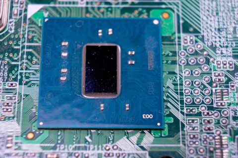


Power Integrity Analysis for Your Power Delivery Network


Designing PCBs to have stable power output is as much an art as it is a science. Power integrity analysis and simulation is all about verifying a design will deliver the required power, but also that the delivered power will be stable. This idea that a power supply might not deliver stable power is not necessarily related to the power supply, it's related to the design of the PDN on the PCB. The structure of a PCB, the elements used to store and deliver power, and the characteristics of modern integrated circuits and regulators can create power delivery problems. Some basic simulation tools will be useful for identifying potential glitches in a power delivery network, as well as qualifying design choices that might affect power integrity.
Before getting into how to analyze a PDN in a PCB, it's important to know what to analyze. There are three primary forms of noise, and multiple sources of power loss and radiation, that can interfere with power delivery and the functionality of components. We'll examine these points in this article, and briefly discuss how they can be identified.
Power Integrity Problems to Identify in Your PCB Layout
There are a few places to look for power integrity problems in your PCB's power distribution network. These points can be investigated both in pre-layout simulations, post-layout simulations (AC or DC), or from measurements:
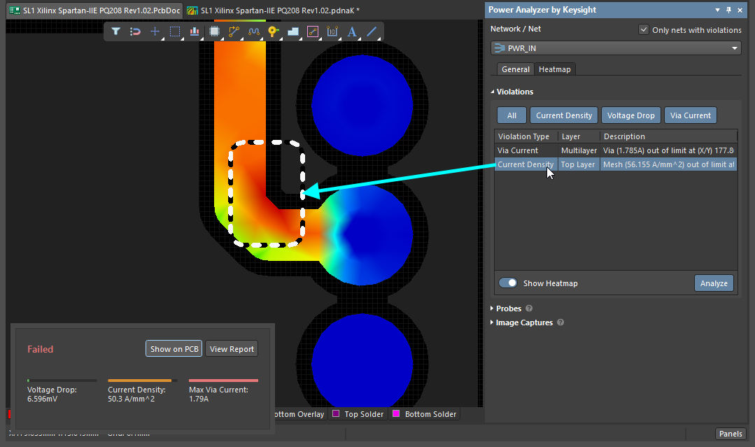
- DC power loss: Because all conductors have nonzero resistance, there will be some loss in voltage across the conductors in the PDN. Post-layout This cannot be measured in a finished PCB without placing copious test points, but a PDN analyzer tools will show you areas with high power dissipation. Voltage drop across a PDN can also be seen in a heat map.
- High PDN impedance: Like any other electrical element, the complex structure of a PDN has some capacitance and inductance, creating a complex PDN impedance spectrum. The PDN impedance needs to be kept low to prevent a transient current drawn into the PDN from being seen as large voltage fluctuations at the power pin of an IC.
- Ripple on the DC power bus: Here, we're not referring to residual ripple from a rectifier bridge. We're worried about the voltage fluctuation seen at an integrated circuit as it draws current into the power bus (supply bounce) or sinks current into a ground plane (ground bounce). This is related to the PDN impedance via Ohm's law. There will always be a small amount of ripple on the DC power bus, but as long as it is small it will not interfere with the operation of components.
- Radiated EMI from a PDN due to high impedance: High impedance does more than create a ripple on the DC power bus, it can also create strong EMI from specific areas of the board that have high impedance.
Gathering power integrity measurements can be as simple as using an oscilloscope to spot glitches on the power bus while a board is operational, or it can involve a VNA measurement to determine the PDN impedance spectrum. Simulations are generally confined to two areas during the design process, but simulations are an important of power integrity analysis.
Pre-layout Simulations
At the schematic level, you can't totally simulate the real structure of a PDN and the impedance it creates, you have to approximate it using circuit models. However, you can simulate things like AC-DC conversion (rectification), DC-DC conversion, and how much noise reaches loads in the system. These simulations can get rather complex, but overall they are important as a first check of power stability in circuit design. Your schematic will need either SPICE subcircuit models for your specific components, or you'll need an equivalent circuit model built from generic components.
DC power integrity is not typically performed in the pre-layout phase because DC power loss depends so heavily on the shape of conductors. Some preliminary analysis can be performed based on thermal limitations as defined in the IPC-2221 and IPC-2152 standards, where the goal is to size conductors carrying DC current or AC power at high current.
- Learn more about thermal analysis in DC power integrity with IPC-2221
- Learn more about using IPC-2152 to relate temperature rise and average current
AC power integrity can be examined in the pre-layout phase using SPICE simulations. In SPICE, the particular points in the PCB layout have to be modeled phenomenologically in a schematic sheet. You can place decoupling capacitor arrays for a power rail, but you will have to include via parasitic inductance and plane capacitance as part of the model. A transient analysis simulation can then be used to estimate the level of power rail noise superimposed on a target DC voltage for a given edge rate in an idealized switching I/O buffer. To learn more, watch the following video.
Post-layout Simulations
Post-layout power integrity simulations can be performed in DC and AC. As was mentioned above, DC power integrity focuses on power drop across conductors in the PCB layout, while AC power integrity focuses on predicting power fluctuations when current is drawn from the PDN by devices in the PCB.
DC power distribution and IR drop in a real PDN can be determined with a DC simulation involving resistance calculations. PDN analysis utilities are used to spot points in a PDN where voltage drops are rather large. For low power boards, this may not be necessary as long as sufficiently large power and ground plane conductors are used in the board. However, for something like a motor or LED controller, large current in a high resistance portion of the PDN can create a hot spot with non-negligible DC voltage drop. This can be spotted the voltage and current distribution outputs from a PDN analysis simulator.
Ideal potential differences in your ground plane should reach sub-mV levels. A difference in ground plane potential as small as 1 mV can interfere with sensitive DC or analog measurements, but this will certainly not be large enough to cause glitches or errors in digital circuits. Whether you actually notice such a problem depends on what you are sourcing or measuring. Noise induced by power supply-dependent fluctuations in the ground potential can be reduced by using a large capacitor across the power supply outputs or across the power and ground plane connections to the power supply.
AC PDN impedance is difficult to simulate directly as a real PDN is a multiport network and is described using an impedance matrix (i.e., Z-parameters). Field solver utilities are needed for these AC simulations from a finished PCB layout. Large PDN impedance not only creates a large voltage fluctuation seen at components, it can also create excessively large radiated EMI, which can jeopardize the product's EMC certification. For a tutorial on this point, take a look at this article.
Measurements
The primary PDN measurement is an impedance measurement, and in some cases a near-field EMI measurement. The two are related, as I've discussed above. For PDN impedance, a spectrum analyzer is normally used and compared to PDN impedance simulation results (Z-parameters). For EMI, a simple first check during operation is to use a high bandwidth oscilloscope with a low impedance, low attenuation ratio near-field probe to check for near-field emission during operation.
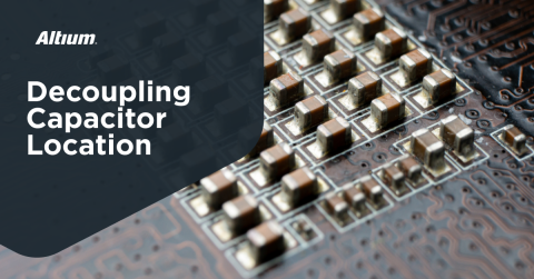
A high PDN impedance can explain large voltage fluctuations and radiated near-field EMI seen on the power bus while a board is operational. To reduce PDN impedance, you can only focus on specific frequency ranges using decoupling capacitors. Due to self-resonance in real capacitors, the PDN impedance cannot be brought sufficiently low at all frequencies. Therefore, plane capacitance is also needed. Read more about designing to low PDN impedance in this article.
Brief Design Guidelines to Ensure Power Integrity
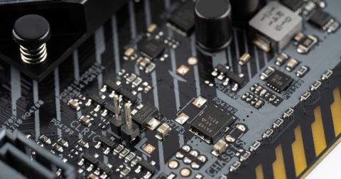
To summarize, power integrity involves checking that the power seen at your components is equal to the value you intended to output from your power regulator. In addition, as the board runs at full power and at high speeds, you need to check that the DC voltage in the PDN does not exhibit large fluctuations. Going further to reduce noise created by grounding problems and ensuring power integrity throughout your device depends in part on the type of power supply you use. For example, a switching power supply generates its own noise due to the high current it draws during switching; this noise is spread out up to MHz levels and can be quite noticeable in high current regulators. Unregulated power supplies output significant ripple in addition to their intended power output.
These variations cannot be solved completely at the PCB level, although a can make an attempt to filter out noise at the switching frequencies. You should always use best design practices to protect critical signal traces and power rails from EMI, regardless of whether this EMI originates from other components on a board, from a power supply, or externally.
Finally, ground bounce can arise for similar reasons as power bus ripple in a PCB due to parasitic inductance seen by signals being sunk into the ground plane. Vias have some natural inductance (usually at the nH level) which, together with package inductance, creates a transient response that can be seen on an I/O when multiple I/Os drawing from the same power rail switch simultaneously (thus it is called simultaneous switching noise and is sometimes confused with crosstalk).
According to Ohm’s law, this requires that the ground potential increase near the via, i.e., the ground potential seen at that IC is greater than that seen at neighboring ICs. This is the essence of ground bounce, thus the need for bypass caps to provide stable power for fast switching I/Os.
Identifying power integrity problems, their influence on signal integrity, and determining the best options for correcting them takes PCB design software with the best simulation and analysis tools on the market. Altium Designer® contains all of these features and many more in a single interface. The signal integrity tools come standard with Altium, and a powerful PDN Analyzer™ is available as an add-on that is conveniently available within the program. When you're ready to send your design into your manufacturer, use the Altium 365 platform to share your design files and stay productive.
We have only scratched the surface of what’s possible with Altium Designer on Altium 365. Start your free trial of Altium Designer + Altium 365 today.

关于作者
Related Technical Documentation
相关资源
目录
从设计到发布,全程无阻碍
- 让评审始终关联到正确的版本
- 减少交接中的混乱和返工
- 更早发现采购与发布风险
- 可独立工作,按需共享
开始使用
Thank you, you are now subscribed to updates.


 沪公网安备 31010502006411号