


Termination Methods in High Speed and High Frequency PCBs


The topic of termination will inevitably come up when dealing with high-speed digital systems. Most digital systems have at least one standardized high-speed interface, or possibly fast GPIOs that produce fast edge rate signals. Advanced systems will have many standardized interfaces which also have termination applied, normally on the semiconductor die. If you determine that you actually need termination, what method should be used?
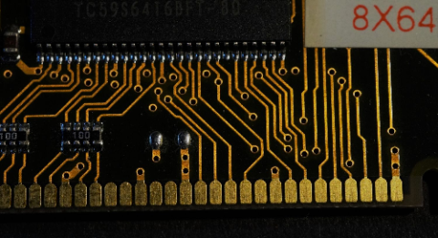
As it turns out, application of discrete terminators is not very common in most digital systems because so many components implement standardized buses for digital communication. But if you are dealing with advanced components that have fast I/Os, then you might need to manually apply termination with discrete components. The other instance where this arises is with specialty logic, such as is sometimes used in certain processors and FPGAs. Finally, there is the matter of RF termination, which is very different from termination digital systems.
When and How to Apply Termination
As was mentioned above, there is a narrow range of cases where termination with discrete components needs to be manually applied.
- Your interface does not have an impedance specification
- Your data sheets state that manual termination is needed
- Your interface specification demands specific termination (e.g., DDR, Bob Smith termination in Ethernet)
RF and digital impedance matching are somewhat different. Overall, the goal is the same: the signal sent into a transmission line should experience minimal loss during propagation and be registered at the correct voltage/power level by the receiving component. The table below compares termination methods used in digital and RF:
|
Digital channel |
RF channel |
|
|
Termination bandwidth |
Requires broadband termination circuit |
Requires narrowband termination circuit |
|
Power loss |
Some power loss is acceptable in certain cases |
Prefer to have no power loss in the passband |
|
Applicable range |
Circuit designs work up to few GHz bandwidths |
Circuit designs are accurate up to few GHz |
|
Standardization |
Usually On-die in standardized interfaces |
High GHz components place termination on-die |
The next point to understand is the proper selection of a termination method for your particular system. The sections below provide brief overviews and links to resources about the various types of terminations that can be used in single ended, differential, and RF interconnects.
Series Termination
This termination method involves placing a series resistor right at the driver's output pin. Technically, transmission lines are linear systems and a series resistor could be put anywhere along the interconnect. However, it is preferable to place the series resistor right at the driver output as this provides most accurate scaling of the output signal and the correct reflection suppression.
- Series Termination Resistor Calculation
- Damping and Reflection Transfer with a Series Termination Resistor
Series resistor values needed for termination can be difficult to determine as the required data is not always present in a datasheet. Instead, it needs to be determined from a known good IBIS model for the driving pin, or it needs to be determined through measurement. Therefore, it is sometimes more desirable to use parallel termination.
Parallel Termination
Parallel termination is used to suppress reflection off of a receiver while also ensuring the full scale voltage is received by the load’s input pin. Therefore, it needs to be placed right at the input pin on the load component, and the value of the resistor is set to be equal to the transmission line’s impedance.
In some special cases, parallel termination and series termination can be used together on the same interconnect, but this is not common. This is more often found in specialty logic, where the output signal level may need to be intentionally shifted down to a lower voltage, but not necessarily with a perfectly matched series resistor. Another instance is where a designer attempts to suppress ground bounce by placing a series resistor for damping, but the reflection off the load is still suppressed with parallel termination.
Thevenin, Pull-Up, and AC Termination
Thevenin termination, pull-up termination, and AC termination are all types of parallel terminations applied at the input pin of a receiving component. They essentially perform the same function as simple parallel termination with a resistor, but with some additional consequences.
- Thevenin - adjusts the voltage level and draws power from an alternative supply voltage
- Pull-up - forces signal to switch around some terminating voltage level; can be used for logic inversion
- AC termination - limits channel bandwidth to lower frequencies and provides a filtering function

Among these three types of terminations, Thevenin and pull-up are used more often. You are more likely to see these implemented on the semiconductor die rather than with discretes. If used with discretes, it is probably a specialty logic case. All three terminations can be found in differential interfaces as part of split termination.
RF Termination
The use of RF termination essentially involves the placement of filters at the output of a driver or at the input of a receiver/load such that the output impedance from a source hits a target impedance. RF impedance matching circuits should ideally have zero resistance, meaning they should only use reactive components. The reason is that we would prefer to not lose any power as a signal interacts with the impedance matching network.
Resistors are broadband terminating components, therefore we want to use them with broadband signals like digital signals. Reactive impedance matching networks produce impedance matching only within a certain bandwidth:
- Reactive components termination circuits create high-Q or low-Q passbands
- Multiple reactive components can be combined in stages to produce higher order filters
- Some circuits will have ripple in their passband, which depends on the termination network topology
Another method that does not involve the use of discretes is the use of transmission line sections. These sections only apply impedance matching in very high-Q bandwidths and are best used with harmonic signals. To see why these points are important, read the links below.
- Quarter-Wave Transformer Design For Real and Reactive Loads
- Impedance Matching Network S-Parameters Simulation
- How to Design an RF Trace Taper for Impedance Matching
Above a few GHz, termination with discrete components will not function as designed due to the presence of parasitics. This is why components operating at many GHz tend to place impedance matching elements directly on the semiconductor die so that output pins will match directly to 50 Ohms. Up to a few GHz, the placement and values used in discrete components needs to be simulated and measured.
No matter what type of impedance matching or termination method you need to design, you can create circuits and design PCBs with the industry’s best electronics design features in Altium Designer®. To implement collaboration in today’s cross-disciplinary environment, innovative companies are using the Altium 365™ platform to easily share design data and put projects into manufacturing.
We have only scratched the surface of what’s possible with Altium Designer on Altium 365. Start your free trial of Altium Designer + Altium 365 today.

关于作者
Related Technical Documentation
相关资源
目录
从设计到发布,全程无阻碍
- 让评审始终关联到正确的版本
- 减少交接中的混乱和返工
- 更早发现采购与发布风险
- 可独立工作,按需共享
开始使用
Thank you, you are now subscribed to updates.


 沪公网安备 31010502006411号