射频(RF)设计在高频下运行,因此需要精密的布局和布线以防止出现信号完整性问题。 RF PCB布局有时可能还包含带有数字元件的线段,精密的布局有助于防止RF和数字信号之间发生干扰。浏览我们的资源库,了解有关RF PCB设计、布局、布线和信号完整性的更多信息。
Coaxial probe feeds can be used to connect to your patch antenna. See how this works in this design example.
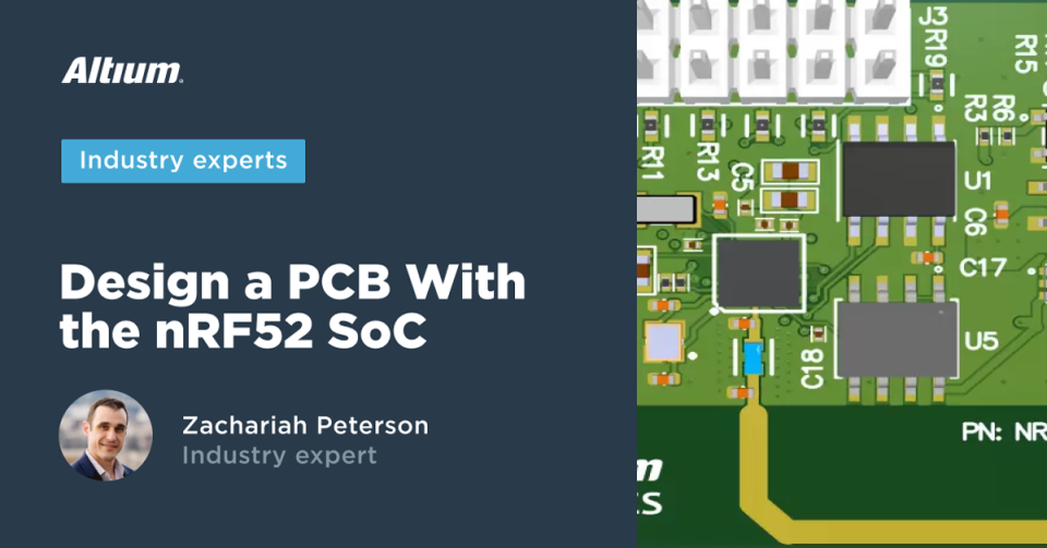
See how to get started with the nRF52 in a PCB layout. We’ll show how to use the fine-pitch BGA package version of this component.
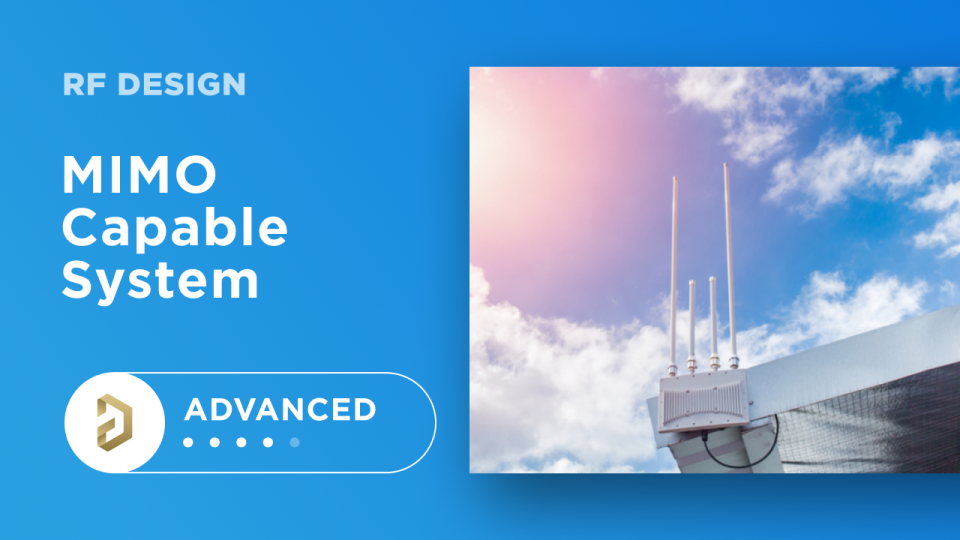
在射频领域运行的高级产品越来越多地使用MIMO天线阵列来提供高数据吞吐量并服务于多个终端用户。
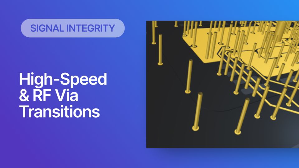
High speed PCBs and RF PCBs often need to make via transitions that carry signals between layers. We’ll look at how to design these transitions in this article.
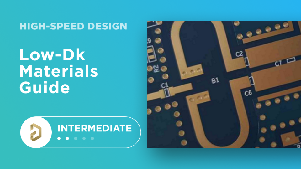
Low-Dk PCB materials are often recommended for high-speed PCB design, but do you always need these? We’ll examine this question.
Take your vehicle’s connectivity to the next level with V2X communication standards. Designing these systems may be easier than you think.