射频(RF)设计在高频下运行,因此需要精密的布局和布线以防止出现信号完整性问题。 RF PCB布局有时可能还包含带有数字元件的线段,精密的布局有助于防止RF和数字信号之间发生干扰。浏览我们的资源库,了解有关RF PCB设计、布局、布线和信号完整性的更多信息。
PCB 阻抗表显示了特定层上走线阻抗的值,但不包括设计师选择的材料或堆叠顺序。
PTFE (Teflon) PCB materials are sometimes seen as the magic bullet for your RF PCB stackups. Make sure you choose the right type of PTFE-based material for your design.
If you work in the electronics industry or in research, there’s a chance that simulations are a regular part of
Advanced car radar systems rely on large virtual arrays for high-resolution imaging, long range, and/or tracking of multiple objects.
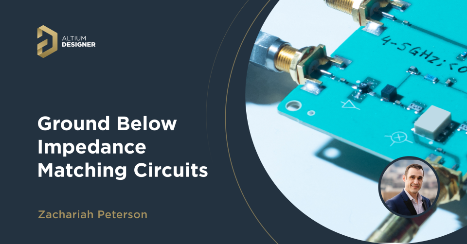
Impedance matching networks in a PCB layout might need to have ground cleared from them. We’ll explore when to remove ground in this short guide.
SMA edge connector footprints sometimes require ground clearance below the connector’s coaxial pin. We’ll show why this can arise and how to qualify the need for ground clearance.