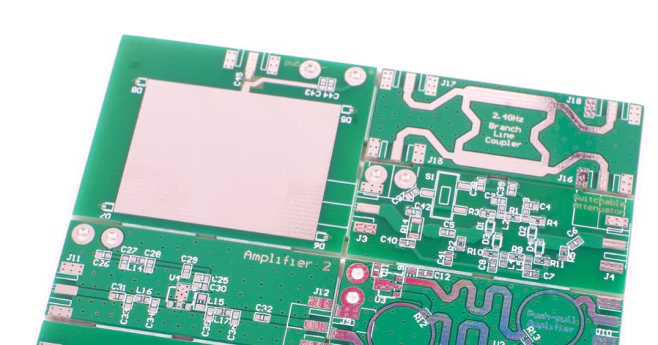
射频(RF)设计在高频下运行,因此需要精密的布局和布线以防止出现信号完整性问题。 RF PCB布局有时可能还包含带有数字元件的线段,精密的布局有助于防止RF和数字信号之间发生干扰。浏览我们的资源库,了解有关RF PCB设计、布局、布线和信号完整性的更多信息。
The simple answer is “no,” all antennas will have a ground plane somewhere, even if it is not on the PCB.
微带线贴片天线的设计和制造结构简单,在非常高的频率下非常有用。
A patch antenna is simple to design in a PCB. These components are placed above a ground plane and require impedance matching.
As the 5G rollout progresses and researchers continue to discuss 6G, many new 5G-capable products operating in sub-GHz and mmWave
JESD204C provides a standardized interface for RF ADCs with high sample rate, which are now appearing more in commercial space applications.
This article will show how a complex load can be converted to a real load with an impedance transformer for any line length and impedance.