Articles and resources related to PCB Layout: Pads & Vias. Check out Altium.com to learn more about PCB Layout and other relevant topics.
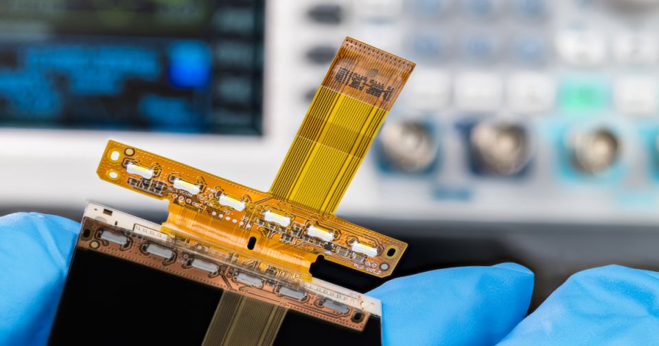
When space is tight, via-in-pad in rigid-flex demands filled vias, clean stackups, and stress control. Learn when to use VIP and when to skip it.
PCB design tips for reliable vias. Learn how via types, copper filling, and fabrication choices improve board reliability and manufacturability.
If you work in the electronics industry or in research, there’s a chance that simulations are a regular part of
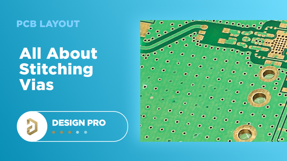
缝合过孔不仅仅是周期性的过孔阵列,它们还提供电源、RF、高速等领域所需的跨层网络连接组。
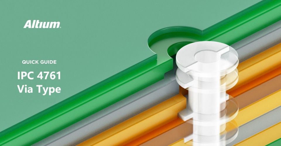
本文档介绍了在 Altium 中根据标准化 IPC-4761 过孔类型支持多种过孔保护方式的可能性,以及每种方式的优点和缺点。
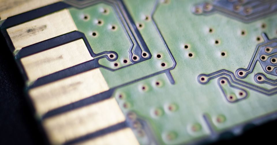
Take a look at the above image of a PCB layout, specifically the vias and drill holes poking through the
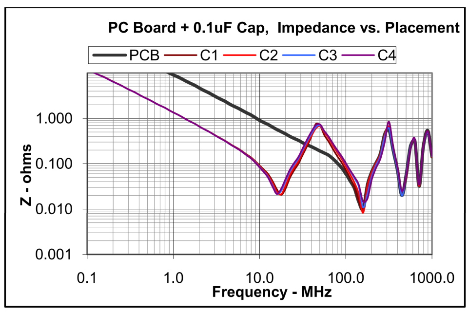
Take a look at traditional PDS impedance versus the “energy flow” view of PDS design. We’ll debunk misleading information that could cause your designs to fail.