Skip to main content
Mobile menu
解决方案
Altium Develop
在 Altium Designer 中设计先进 PCB,可独立设计,也可在需要时连接评审、数据来源和发布协同。
Altium Agile Teams
在多学科电子开发与协作中引入结构化流程,确保效率与速度不受影响。
资源 & 支持中心
Altium 365 免费工具
Gerber Compare
在线 PCB 查看器
了解产品
下载
联系我们
关注微信
扫描二维码
关注Altium微信平台
资源 & 支持中心
用户指南
实战讲堂
学习中心
技术文档
支持中心
常见问题
Altium 社群
社群
Bug提交
创意
教育
学生实验室
Free access to professional PCB design software, training, and learning resources for students
教育者中心
A comprehensive education platform providing curriculum, software, training, and classroom resources for educators
Altium 教育课程
Free college- and university-level PCB design curriculum designed to prepare students for real-world engineering careers
Search Open
Search
Search Close
登录
信号完整性
Main menu
首页
PCB设计
团队协作
元器件创建
PCB数据管理
PCB设计输出和文档
ECAD/MCAD
HDI设计
高速设计
多板设计
PCB布局
PCB布线
PCB供应链
电源完整性
RF设计
刚柔结合板PCB设计
原理图输入
信号完整性
PCB设计仿真/分析
软件
Discover
Develop
敏捷团队
敏捷企业
Altium 365
Altium Designer
资源中心
项目
Altium Academy
工程新闻
指南书
新闻通讯
播客
项目
培训课程
网络研讨会
白皮书
首页
信号完整性
信号完整性
浏览我们的资源库了解更多关于PCB设计和信号完整性。
What is Signal Integrity?
PCB Design Fundamentals
xSignals in Altium
Signal Integrity Stimulus Design Rules
Basics of Signal Integrity Analysis
Overview
指南
网络研讨会
视频
Tech Docs
All Content
Filter
found
Sort by
Most Recent
Most Popular
Title (A-Z)
Title (Z-A)
Role
电气工程师
机械设计工程师
PCB 设计工程师
Software
Altium Develop
Altium Agile 团队
Altium Designer
Altium 365
PLM集成
Octopart
Content Type
指南
视频
网络研讨会
白皮书
播客
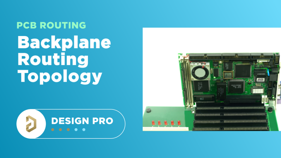
Backplane Routing Topology for Gigabit Copper and Fiber Networks
10 min
Blog
Backplanes are the backbone of modular computing platforms, providing a fabric that interlinks pluggable daughtercards in a single system. The
阅读文章
Silicon Photonics Integration Challenges in PCB Design
7 min
Blog
Silicon photonics will use the same manufacturing processes used in silicon ICs I was honored to meet Richard Soref at
阅读文章
Insertion Loss Deviation or Intersymbol Interference Noise?
11 min
Blog
In a previous blog, I discussed how channel quality is quantified by eye patterns [1]. There, it is explained how
阅读文章
How to Layout a Phase-locked Loop IC in Your RF PCB
8 min
Thought Leadership
As part of telecom systems, radio systems, and other RF devices requiring frequency synthesis, phase-locked loops play an important role
阅读文章
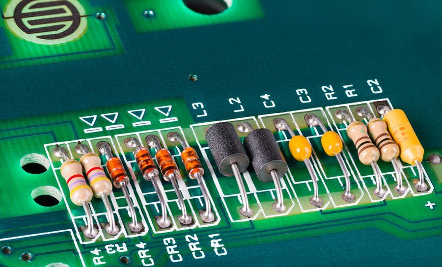
The Role of a Decoupling, Inductors, and Resistance in a PDN
9 min
Thought Leadership
What is the role of a RF decoupling capacitor? Do I need a decoupling circuit for my PCB? Some designers might overlook the role of a decoupling, inductance, and resistance when designing their power distribution network.
阅读文章
解耦电容计算:您应该为数字IC使用什么尺寸?
1 min
Blog
这些去耦电容的尺寸选得合适吗? 在PCB设计指南中,包括高速数字设计“大师”们经常提到的一点是,需要找到合适的去耦电容尺寸。这有时候是在没有完全理解这些电容在PDN中应该做什么,以及它们在确保电源完整性方面的作用的情况下被提及的。我还看到许多应用说明书默认使用几十年前的指南,即在数字集成电路的电源和地脚之间放置三个电容(通常是1 nF、10 nF和100 nF,或类似这样的配置)。在过去,这可能是足够的;快速数字组件中出现的电源完整性问题并不足以干扰核心电压,所以三个电容完成的工作还算不错。 今天的快速集成电路具有多个输出和低核心电压(低至1.0V),与昔日的较慢组件相比,它们有着更严格的噪声限制。更严格的噪声限制意味着需要更精确的去耦。既然如此,任何与当今相当强大的MCU和许多其他数字组件打交道的设计师都需要知道如何正确地选择去耦电容的大小。那么,最佳的做法是什么呢?一般来说,有两种方法可以做到这一点。让我们来看看这两种方法,了解如何计算去耦电容的值,以及为什么旧有的三个去耦电容的神话在现代高速数字设计中不再适用。 理解等效电容模型 在我们开始确定数字设计所需的去耦电容大小之前,你需要了解电容器的基本电路模型。尽管我们很希望认为电容器的行为完全符合理论,但实际情况并非如此。所有的电容器在引线上都有一定的电感,这定义了它们的阻抗谱,这种阻抗谱是以串联RLC网络经验模型来表示的: 用于模拟电容器的等效RLC电路 在这个模型中,ESR 和 ESL 分别是等效串联电阻和等效串联电感。C 的值可以按照元件数据表中引用的电容量来取。最后,R 的值考虑了构成电容器的电介质的电导。这解释了任何电容器在充电后从其电路中移除时发生的瞬态泄漏。这个值通常足够大,可以忽略。 在这个模型中(忽略 R),值 (ESR/(2*ESL)) 是等效电路的阻尼常数,假设连接到电路两端的负载为 0
阅读文章
Symmetric Stripline Inductance or Impedance Calculators and Formulas
6 min
Blog
In a previous article, we looked at the inconsistencies that can arise when using different calculators to compute the impedance
阅读文章
Pagination
First page
« First
Previous page
‹‹
页面
28
当前页面
29
页面
30
页面
31
页面
32
页面
33
Next page
››
Last page
Last »









 沪公网安备 31010502006411号